ADC12DL080CIVS/NOPB
ActiveDUAL-CHANNEL, 12-BIT, 80-MSPS, 600-MHZ INPUT BANDWIDTH ANALOG-TO-DIGITAL CONVERTER (ADC)
Deep-Dive with AI
Search across all available documentation for this part.
ADC12DL080CIVS/NOPB
ActiveDUAL-CHANNEL, 12-BIT, 80-MSPS, 600-MHZ INPUT BANDWIDTH ANALOG-TO-DIGITAL CONVERTER (ADC)
Technical Specifications
Parameters and characteristics for this part
| Specification | ADC12DL080CIVS/NOPB |
|---|---|
| Architecture | Pipelined |
| Configuration | S/H-ADC |
| Data Interface | Parallel |
| Features | Simultaneous Sampling |
| Input Type | Differential |
| Mounting Type | Surface Mount |
| Number of A/D Converters | 2 |
| Number of Bits | 12 |
| Number of Inputs | 2 |
| Operating Temperature [Max] | 85 °C |
| Operating Temperature [Min] | -40 °C |
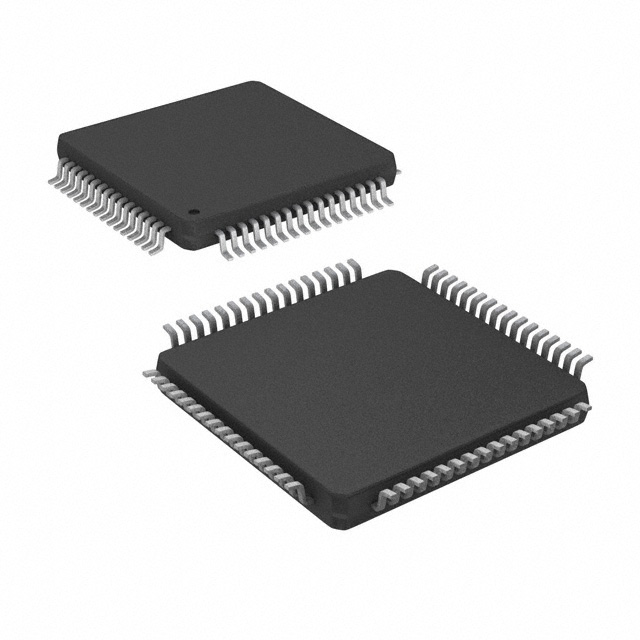
| Package / Case | 64-TQFP |
| Ratio - S/H:ADC | 1:1 |
| Reference Type | Internal, External |
| Sampling Rate (Per Second) | 80 M |
| Supplier Device Package | 64-TQFP (10x10) |
| Voltage - Supply, Analog [Max] | 3.6 V |
| Voltage - Supply, Analog [Min] | 3 V |
| Voltage - Supply, Digital [Max] | 3.6 V |
| Voltage - Supply, Digital [Min] | 2.4 V |
Pricing
Prices provided here are for design reference only. For realtime values and availability, please visit the distributors directly
ADC12DL080 Series
Dual-Channel, 12-Bit, 80-MSPS, 600-MHz Input Bandwidth Analog-to-Digital Converter (ADC)
| Part | Ratio - S/H:ADC | Sampling Rate (Per Second) | Mounting Type | Architecture | Voltage - Supply, Analog [Max] | Voltage - Supply, Analog [Min] | Reference Type | Data Interface | Operating Temperature [Min] | Operating Temperature [Max] | Number of Inputs | Input Type | Supplier Device Package | Features | Configuration | Number of A/D Converters | Voltage - Supply, Digital [Max] | Voltage - Supply, Digital [Min] | Package / Case | Number of Bits |
|---|---|---|---|---|---|---|---|---|---|---|---|---|---|---|---|---|---|---|---|---|
Texas Instruments ADC12DL080CIVS/NOPBThe ADC12DL080 is a dual, low power monolithic CMOS analog-to-digital converter capable of converting analog input signals into 12-bit digital words at 80 Megasamples per second (MSPS). This converter uses a differential, pipeline architecture with digital error correction and an on-chip sample-and-hold circuit to minimize power consumption while providing excellent dynamic performance and a 600 MHz Full Power Bandwidth. Operating on a single +3.3V power supply, the ADC12DL080 achieves 11.0 effective bits at Nyquist and consumes just 447mW at 80 MSPS. The Power Down feature reduces power consumption to 50 mW.
The differential inputs provide a full scale differential input swing equal to 2 times VREFwith the possibility of a single-ended input. Full use of the differential input is recommended for optimum performance. Duty cycle stabilization and output data format are selectable. The output data can be set for offset binary or two's complement.
To ease interfacing to lower voltage systems, the digital output driver power pins of the ADC12DL080 can be connected to a separate supply voltage in the range of 2.4V to the analog supply voltage. This device is available in the 64-lead TQFP package and will operate over the industrial temperature range of −40°C to +85°C. An evaluation board is available to ease the evaluation process.
The ADC12DL080 is a dual, low power monolithic CMOS analog-to-digital converter capable of converting analog input signals into 12-bit digital words at 80 Megasamples per second (MSPS). This converter uses a differential, pipeline architecture with digital error correction and an on-chip sample-and-hold circuit to minimize power consumption while providing excellent dynamic performance and a 600 MHz Full Power Bandwidth. Operating on a single +3.3V power supply, the ADC12DL080 achieves 11.0 effective bits at Nyquist and consumes just 447mW at 80 MSPS. The Power Down feature reduces power consumption to 50 mW.
The differential inputs provide a full scale differential input swing equal to 2 times VREFwith the possibility of a single-ended input. Full use of the differential input is recommended for optimum performance. Duty cycle stabilization and output data format are selectable. The output data can be set for offset binary or two's complement.
To ease interfacing to lower voltage systems, the digital output driver power pins of the ADC12DL080 can be connected to a separate supply voltage in the range of 2.4V to the analog supply voltage. This device is available in the 64-lead TQFP package and will operate over the industrial temperature range of −40°C to +85°C. An evaluation board is available to ease the evaluation process. | 1:1 | 80 M | Surface Mount | Pipelined | 3.6 V | 3 V | External, Internal | Parallel | -40 °C | 85 °C | 2 | Differential | 64-TQFP (10x10) | Simultaneous Sampling | S/H-ADC | 2 | 3.6 V | 2.4 V | 64-TQFP | 12 |
Description
General part information
ADC12DL080 Series
The ADC12DL080 is a dual, low power monolithic CMOS analog-to-digital converter capable of converting analog input signals into 12-bit digital words at 80 Megasamples per second (MSPS). This converter uses a differential, pipeline architecture with digital error correction and an on-chip sample-and-hold circuit to minimize power consumption while providing excellent dynamic performance and a 600 MHz Full Power Bandwidth. Operating on a single +3.3V power supply, the ADC12DL080 achieves 11.0 effective bits at Nyquist and consumes just 447mW at 80 MSPS. The Power Down feature reduces power consumption to 50 mW.
The differential inputs provide a full scale differential input swing equal to 2 times VREFwith the possibility of a single-ended input. Full use of the differential input is recommended for optimum performance. Duty cycle stabilization and output data format are selectable. The output data can be set for offset binary or two's complement.
To ease interfacing to lower voltage systems, the digital output driver power pins of the ADC12DL080 can be connected to a separate supply voltage in the range of 2.4V to the analog supply voltage. This device is available in the 64-lead TQFP package and will operate over the industrial temperature range of −40°C to +85°C. An evaluation board is available to ease the evaluation process.