ADC16V130CISQ/NOPB
Active16-BIT, 130-MSPS ANALOG-TO-DIGITAL CONVERTER (ADC)
Deep-Dive with AI
Search across all available documentation for this part.
ADC16V130CISQ/NOPB
Active16-BIT, 130-MSPS ANALOG-TO-DIGITAL CONVERTER (ADC)
Technical Specifications
Parameters and characteristics commom to parts in this series
| Specification | ADC16V130CISQ/NOPB | ADC16V130 Series |
|---|---|---|
| Architecture | Pipelined | Pipelined |
| Configuration | S/H-ADC | S/H-ADC |
| Data Interface | LVDS - Parallel | LVDS - Parallel |
| Input Type | Differential | Differential |
| Mounting Type | Surface Mount | Surface Mount |
| Number of A/D Converters | 1 | 1 |
| Number of Bits | 16 bits | 16 bits |
| Number of Inputs | 1 | 1 |
| Operating Temperature [Max] | 85 °C | 85 °C |
| Operating Temperature [Min] | -40 °C | -40 °C |
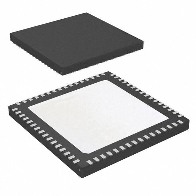
| Package / Case | 64-WFQFN Exposed Pad | 64-WFQFN Exposed Pad |
| Ratio - S/H:ADC | 1:1 | 1:1 |
| Reference Type | Internal, External | Internal, External |
| Sampling Rate (Per Second) | 130 M | 130 M |
| Supplier Device Package | 64-WQFN (9x9) | 64-WQFN (9x9) |
| Voltage - Supply, Analog [Max] | 3.6 V | 3.6 V |
| Voltage - Supply, Analog [Min] | 1.7 V | 1.7 V |
| Voltage - Supply, Digital [Max] | 1.9 V | 1.9 V |
| Voltage - Supply, Digital [Min] | 1.7 V | 1.7 V |
Pricing
Prices provided here are for design reference only. For realtime values and availability, please visit the distributors directly
ADC16V130 Series
16-Bit, 130-MSPS Analog-to-Digital Converter (ADC)
| Part | Data Interface | Package / Case | Configuration | Reference Type | Voltage - Supply, Digital [Min] | Voltage - Supply, Digital [Max] | Mounting Type | Operating Temperature [Min] | Operating Temperature [Max] | Ratio - S/H:ADC | Number of Inputs | Architecture | Number of Bits | Voltage - Supply, Analog [Min] | Voltage - Supply, Analog [Max] | Number of A/D Converters | Supplier Device Package | Sampling Rate (Per Second) | Input Type |
|---|---|---|---|---|---|---|---|---|---|---|---|---|---|---|---|---|---|---|---|
Texas Instruments ADC16V130CISQX/NOPBThe ADC16V130 is a monolithic high performance CMOS analog-to-digital converter capable of converting analog input signals into 16-bit digital words at rates up to 130 Mega Samples Per Second (MSPS). This converter uses a differential, pipelined architecture with digital error correction and an on-chip sample-and-hold circuit to minimize power consumption and external component count while providing excellent dynamic performance. Automatic power-up calibration enables excellent dynamic performance and reduces part-to-part variation, and the ADC16V130 could be re-calibrated at any time by asserting and then de-asserting power-down. An integrated low noise and stable voltage reference and differential reference buffer amplifier easies board level design. On-chip duty cycle stabilizer with low additive jitter allows wide duty cycle range of input clock without compromising its dynamic performance. A unique sample-and-hold stage yields a full-power bandwidth of 1.4 GHz. The digital data is provided via full data rate LVDS outputs – making possible the 64-pin, 9mm x 9mm WQFN package. The ADC16V130 operates on dual power supplies +1.8V and +3.0V with a power-down feature to reduce the power consumption to very low levels while allowing fast recovery to full operation.
The ADC16V130 is a monolithic high performance CMOS analog-to-digital converter capable of converting analog input signals into 16-bit digital words at rates up to 130 Mega Samples Per Second (MSPS). This converter uses a differential, pipelined architecture with digital error correction and an on-chip sample-and-hold circuit to minimize power consumption and external component count while providing excellent dynamic performance. Automatic power-up calibration enables excellent dynamic performance and reduces part-to-part variation, and the ADC16V130 could be re-calibrated at any time by asserting and then de-asserting power-down. An integrated low noise and stable voltage reference and differential reference buffer amplifier easies board level design. On-chip duty cycle stabilizer with low additive jitter allows wide duty cycle range of input clock without compromising its dynamic performance. A unique sample-and-hold stage yields a full-power bandwidth of 1.4 GHz. The digital data is provided via full data rate LVDS outputs – making possible the 64-pin, 9mm x 9mm WQFN package. The ADC16V130 operates on dual power supplies +1.8V and +3.0V with a power-down feature to reduce the power consumption to very low levels while allowing fast recovery to full operation. | LVDS - Parallel | 64-WFQFN Exposed Pad | S/H-ADC | External, Internal | 1.7 V | 1.9 V | Surface Mount | -40 °C | 85 °C | 1:1 | 1 | Pipelined | 16 bits | 1.7 V | 3.6 V | 1 | 64-WQFN (9x9) | 130 M | Differential |
Texas Instruments ADC16V130CISQE/NOPBThe ADC16V130 is a monolithic high performance CMOS analog-to-digital converter capable of converting analog input signals into 16-bit digital words at rates up to 130 Mega Samples Per Second (MSPS). This converter uses a differential, pipelined architecture with digital error correction and an on-chip sample-and-hold circuit to minimize power consumption and external component count while providing excellent dynamic performance. Automatic power-up calibration enables excellent dynamic performance and reduces part-to-part variation, and the ADC16V130 could be re-calibrated at any time by asserting and then de-asserting power-down. An integrated low noise and stable voltage reference and differential reference buffer amplifier easies board level design. On-chip duty cycle stabilizer with low additive jitter allows wide duty cycle range of input clock without compromising its dynamic performance. A unique sample-and-hold stage yields a full-power bandwidth of 1.4 GHz. The digital data is provided via full data rate LVDS outputs – making possible the 64-pin, 9mm x 9mm WQFN package. The ADC16V130 operates on dual power supplies +1.8V and +3.0V with a power-down feature to reduce the power consumption to very low levels while allowing fast recovery to full operation.
The ADC16V130 is a monolithic high performance CMOS analog-to-digital converter capable of converting analog input signals into 16-bit digital words at rates up to 130 Mega Samples Per Second (MSPS). This converter uses a differential, pipelined architecture with digital error correction and an on-chip sample-and-hold circuit to minimize power consumption and external component count while providing excellent dynamic performance. Automatic power-up calibration enables excellent dynamic performance and reduces part-to-part variation, and the ADC16V130 could be re-calibrated at any time by asserting and then de-asserting power-down. An integrated low noise and stable voltage reference and differential reference buffer amplifier easies board level design. On-chip duty cycle stabilizer with low additive jitter allows wide duty cycle range of input clock without compromising its dynamic performance. A unique sample-and-hold stage yields a full-power bandwidth of 1.4 GHz. The digital data is provided via full data rate LVDS outputs – making possible the 64-pin, 9mm x 9mm WQFN package. The ADC16V130 operates on dual power supplies +1.8V and +3.0V with a power-down feature to reduce the power consumption to very low levels while allowing fast recovery to full operation. | LVDS - Parallel | 64-WFQFN Exposed Pad | S/H-ADC | External, Internal | 1.7 V | 1.9 V | Surface Mount | -40 °C | 85 °C | 1:1 | 1 | Pipelined | 16 bits | 1.7 V | 3.6 V | 1 | 64-WQFN (9x9) | 130 M | Differential |
Texas Instruments ADC16V130CISQ/NOPBThe ADC16V130 is a monolithic high performance CMOS analog-to-digital converter capable of converting analog input signals into 16-bit digital words at rates up to 130 Mega Samples Per Second (MSPS). This converter uses a differential, pipelined architecture with digital error correction and an on-chip sample-and-hold circuit to minimize power consumption and external component count while providing excellent dynamic performance. Automatic power-up calibration enables excellent dynamic performance and reduces part-to-part variation, and the ADC16V130 could be re-calibrated at any time by asserting and then de-asserting power-down. An integrated low noise and stable voltage reference and differential reference buffer amplifier easies board level design. On-chip duty cycle stabilizer with low additive jitter allows wide duty cycle range of input clock without compromising its dynamic performance. A unique sample-and-hold stage yields a full-power bandwidth of 1.4 GHz. The digital data is provided via full data rate LVDS outputs – making possible the 64-pin, 9mm x 9mm WQFN package. The ADC16V130 operates on dual power supplies +1.8V and +3.0V with a power-down feature to reduce the power consumption to very low levels while allowing fast recovery to full operation.
The ADC16V130 is a monolithic high performance CMOS analog-to-digital converter capable of converting analog input signals into 16-bit digital words at rates up to 130 Mega Samples Per Second (MSPS). This converter uses a differential, pipelined architecture with digital error correction and an on-chip sample-and-hold circuit to minimize power consumption and external component count while providing excellent dynamic performance. Automatic power-up calibration enables excellent dynamic performance and reduces part-to-part variation, and the ADC16V130 could be re-calibrated at any time by asserting and then de-asserting power-down. An integrated low noise and stable voltage reference and differential reference buffer amplifier easies board level design. On-chip duty cycle stabilizer with low additive jitter allows wide duty cycle range of input clock without compromising its dynamic performance. A unique sample-and-hold stage yields a full-power bandwidth of 1.4 GHz. The digital data is provided via full data rate LVDS outputs – making possible the 64-pin, 9mm x 9mm WQFN package. The ADC16V130 operates on dual power supplies +1.8V and +3.0V with a power-down feature to reduce the power consumption to very low levels while allowing fast recovery to full operation. | LVDS - Parallel | 64-WFQFN Exposed Pad | S/H-ADC | External, Internal | 1.7 V | 1.9 V | Surface Mount | -40 °C | 85 °C | 1:1 | 1 | Pipelined | 16 bits | 1.7 V | 3.6 V | 1 | 64-WQFN (9x9) | 130 M | Differential |
Description
General part information
ADC16V130 Series
The ADC16V130 is a monolithic high performance CMOS analog-to-digital converter capable of converting analog input signals into 16-bit digital words at rates up to 130 Mega Samples Per Second (MSPS). This converter uses a differential, pipelined architecture with digital error correction and an on-chip sample-and-hold circuit to minimize power consumption and external component count while providing excellent dynamic performance. Automatic power-up calibration enables excellent dynamic performance and reduces part-to-part variation, and the ADC16V130 could be re-calibrated at any time by asserting and then de-asserting power-down. An integrated low noise and stable voltage reference and differential reference buffer amplifier easies board level design. On-chip duty cycle stabilizer with low additive jitter allows wide duty cycle range of input clock without compromising its dynamic performance. A unique sample-and-hold stage yields a full-power bandwidth of 1.4 GHz. The digital data is provided via full data rate LVDS outputs – making possible the 64-pin, 9mm x 9mm WQFN package. The ADC16V130 operates on dual power supplies +1.8V and +3.0V with a power-down feature to reduce the power consumption to very low levels while allowing fast recovery to full operation.
The ADC16V130 is a monolithic high performance CMOS analog-to-digital converter capable of converting analog input signals into 16-bit digital words at rates up to 130 Mega Samples Per Second (MSPS). This converter uses a differential, pipelined architecture with digital error correction and an on-chip sample-and-hold circuit to minimize power consumption and external component count while providing excellent dynamic performance. Automatic power-up calibration enables excellent dynamic performance and reduces part-to-part variation, and the ADC16V130 could be re-calibrated at any time by asserting and then de-asserting power-down. An integrated low noise and stable voltage reference and differential reference buffer amplifier easies board level design. On-chip duty cycle stabilizer with low additive jitter allows wide duty cycle range of input clock without compromising its dynamic performance. A unique sample-and-hold stage yields a full-power bandwidth of 1.4 GHz. The digital data is provided via full data rate LVDS outputs – making possible the 64-pin, 9mm x 9mm WQFN package. The ADC16V130 operates on dual power supplies +1.8V and +3.0V with a power-down feature to reduce the power consumption to very low levels while allowing fast recovery to full operation.
Documents
Technical documentation and resources