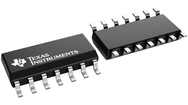
SN74LVC74AQDRG4Q1
ActiveAUTOMOTIVE, DUAL POSITIVE-EDGE-TRIGGERED D-TYPE FLIP-FLOPS WITH CLEAR AND PRESET
SN74LVC74AQDRG4Q1
ActiveAUTOMOTIVE, DUAL POSITIVE-EDGE-TRIGGERED D-TYPE FLIP-FLOPS WITH CLEAR AND PRESET
Description
General part information
74LVC74 Series
The SN74LVC74A dual positive-edge-triggered D-type flip-flop is designed for 2.7-V to 3.6-V VCCoperation.
A low level at the preset (PRE) or clear (CLR) inputs sets or resets the outputs, regardless of the levels of the other inputs. WhenPREandCLRare inactive (high), data at the data (D) input meeting the setup time requirements is transferred to the outputs on the positive-going edge of the clock pulse. Clock triggering occurs at a voltage level and is not directly related to the rise time of the clock pulse. Following the hold-time interval, data at the D input can be changed without affecting the levels at the outputs.
Inputs can be driven from either 3.3 V or 5 V devices. This feature allows the use of this device as a translator in a mixed 3.3 V/5 V system environment.
Technical Specifications
Parameters and characteristics for this part
| Specification | SN74LVC74AQDRG4Q1 |
|---|---|
| Clock Frequency | 150 MHz |
| Current - Output High | 24 mA |
| Current - Output Low | 24 mA |
| Current - Quiescent (Iq) | 10 µA |
| Function | Set(Preset) and Reset |
| Grade | Automotive |
| Input Capacitance | 5 pF |
| Max CL | 50 pF |
| Max Propagation Delay | 5.2 ns |
| Mounting Type | Surface Mount |
| Number of Bits per Element | 1 bits |
| Number of Elements | 2 |
| Operating Temperature (Max) | 125 °C |
| Operating Temperature (Min) | -40 °C |
| Output Type | Complementary |
| Package Length | 0.154 in |
| Package Name | 14-SOIC |
| Package Width | 3.9 mm |
| Qualification | AEC-Q100 |
| Trigger Type | Positive Edge |
| Type | D-Type |
| Voltage - Supply (Maximum) | 3.6 V |
| Voltage - Supply (Minimum) | 2 V |
Pricing
Prices provided here are for design reference only. For realtime values and availability, please visit the distributors directly
Sign in to see pricing
Create a free account to access distributor pricing data.
CAD
3D models and CAD resources for this part
Documents
Technical documentation and resources