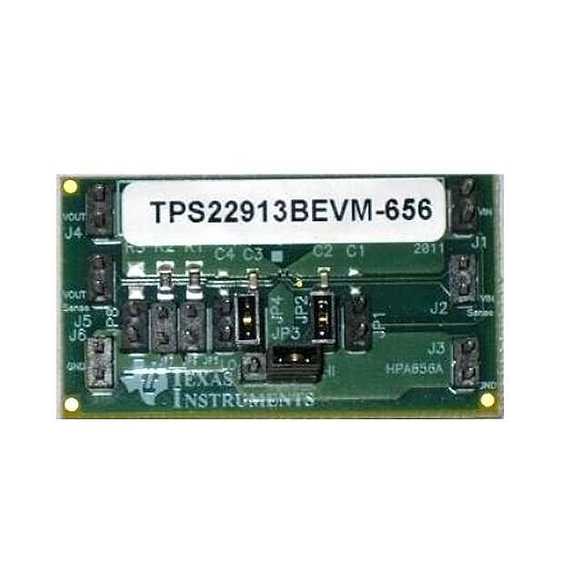
TPS22913BEVM-656
ActiveTexas Instruments
EVAL MODULE FOR TPS22913BE-656
Deep-Dive with AI
Search across all available documentation for this part.
DocumentsDatasheet
TPS22913BEVM-656
ActiveTexas Instruments
EVAL MODULE FOR TPS22913BE-656
Deep-Dive with AI
DocumentsDatasheet
Technical Specifications
Parameters and characteristics commom to parts in this series
| Specification | TPS22913BEVM-656 | TPS22913 Series |
|---|---|---|
| Contents | - | Board(s) |
| Current - Output (Max) | - | 2 A |
| Embedded | False | False |
| Fault Protection | - | Reverse Current, UVLO |
| Features | - | Slew Rate Controlled, Load Discharge |
| Function | Power Distribution Switch (Load Switch) | Power Distribution Switch (Load Switch) |
| Input Type | - | Non-Inverting |
| Interface | - | On/Off |
| Mounting Type | - | Surface Mount |
| Number of Outputs | - | 1 |
| Operating Temperature | - | 85 °C |
| Operating Temperature | - | -40 °C |
| Output Configuration | - | High Side |
| Output Type | - | P-Channel |
| Package / Case | - | 4-XFBGA, DSBGA |
| Primary Attributes | Single Channel, Controlled Turn-ON, Low rON | Single Channel, Controlled Turn-ON, Low rON |
| Primary Attributes | 2 A | 2 A |
| Ratio - Input:Output | - | 1:1 |
| Rds On (Typ) | - | 60 mOhm |
| Supplied Contents | Board(s) | Board(s) |
| Supplier Device Package | - | 4-DSBGA (0.88x0.88) |
| Switch Type | - | General Purpose |
| Type | Power Management | Power Management |
| Utilized IC / Part | TPS22913B | TPS22913C, TPS22913B |
| Voltage - Load | - | 1.4 V |
| Voltage - Load | - | 5.5 V |
| Voltage - Supply (Vcc/Vdd) | - | Not Required |
Pricing
Prices provided here are for design reference only. For realtime values and availability, please visit the distributors directly
TPS22913 Series
5.5-V, 2-A, 60-MΩ LOAD SWITCH WITH OUTPUT DISCHARGE 4-DSBGA -40 TO 85
| Part | Rds On (Typ) | Voltage - Supply (Vcc/Vdd) | Output Type | Switch Type | Operating Temperature [Max] | Operating Temperature [Min] | Mounting Type | Supplier Device Package | Input Type | Voltage - Load [Min] | Voltage - Load [Max] | Number of Outputs | Current - Output (Max) [Max] | Ratio - Input:Output [custom] | Package / Case | Features | Interface | Fault Protection | Output Configuration | Primary Attributes | Primary Attributes | Contents | Utilized IC / Part | Supplied Contents | Function | Embedded | Type |
|---|---|---|---|---|---|---|---|---|---|---|---|---|---|---|---|---|---|---|---|---|---|---|---|---|---|---|---|
Texas Instruments TPS22913BYZVTThe TPS22910A, TPS22912C, and TPS22913B/C are small, low rONload switches with controlled turn on. The device contains a P-channel MOSFET that can operate over an input voltage range of 1.4 V to 5.5 V. The switch is controlled by an on/off input (ON), which is capable of interfacing directly with low-voltage GPIO control signals.
The TPS22910A, TPS22912C, and TPS22913B/C devices provide reverse current protection in ON and OFF states. An internal reverse voltage comparator disables the power-switch when the output voltage (VOUT) is driven higher than the input voltage (VIN), by VRCP, to quickly (10 µs typ) stop the flow of current towards the input side of the switch. Reverse current protection is always active, even when the power-switch is disabled. Additionally, under-voltage lockout (UVLO) protection turns the switch off if the input voltage is too low.
The TPS22913B/C contains a 150-Ω on-chip load resistor for quick output discharge when the switch is turned off.
This family of devices have various slew rate options to avoid inrush current (see for details), are available in an ultra-small, space-saving 4-pin WCSP packages, and are characterized for operation over the free-air temperature range of –40°C to 85°C.
The TPS22910A, TPS22912C, and TPS22913B/C are small, low rONload switches with controlled turn on. The device contains a P-channel MOSFET that can operate over an input voltage range of 1.4 V to 5.5 V. The switch is controlled by an on/off input (ON), which is capable of interfacing directly with low-voltage GPIO control signals.
The TPS22910A, TPS22912C, and TPS22913B/C devices provide reverse current protection in ON and OFF states. An internal reverse voltage comparator disables the power-switch when the output voltage (VOUT) is driven higher than the input voltage (VIN), by VRCP, to quickly (10 µs typ) stop the flow of current towards the input side of the switch. Reverse current protection is always active, even when the power-switch is disabled. Additionally, under-voltage lockout (UVLO) protection turns the switch off if the input voltage is too low.
The TPS22913B/C contains a 150-Ω on-chip load resistor for quick output discharge when the switch is turned off.
This family of devices have various slew rate options to avoid inrush current (see for details), are available in an ultra-small, space-saving 4-pin WCSP packages, and are characterized for operation over the free-air temperature range of –40°C to 85°C. | 60 mOhm | Not Required | P-Channel | General Purpose | 85 °C | -40 °C | Surface Mount | 4-DSBGA (0.88x0.88) | Non-Inverting | 1.4 V | 5.5 V | 1 | 2 A | 1:1 | 4-XFBGA, DSBGA | Load Discharge, Slew Rate Controlled | On/Off | Reverse Current, UVLO | High Side | ||||||||
Texas Instruments TPS22913BYZVRThe TPS22910A, TPS22912C, and TPS22913B/C are small, low rONload switches with controlled turn on. The device contains a P-channel MOSFET that can operate over an input voltage range of 1.4 V to 5.5 V. The switch is controlled by an on/off input (ON), which is capable of interfacing directly with low-voltage GPIO control signals.
The TPS22910A, TPS22912C, and TPS22913B/C devices provide reverse current protection in ON and OFF states. An internal reverse voltage comparator disables the power-switch when the output voltage (VOUT) is driven higher than the input voltage (VIN), by VRCP, to quickly (10 µs typ) stop the flow of current towards the input side of the switch. Reverse current protection is always active, even when the power-switch is disabled. Additionally, under-voltage lockout (UVLO) protection turns the switch off if the input voltage is too low.
The TPS22913B/C contains a 150-Ω on-chip load resistor for quick output discharge when the switch is turned off.
This family of devices have various slew rate options to avoid inrush current (see for details), are available in an ultra-small, space-saving 4-pin WCSP packages, and are characterized for operation over the free-air temperature range of –40°C to 85°C.
The TPS22910A, TPS22912C, and TPS22913B/C are small, low rONload switches with controlled turn on. The device contains a P-channel MOSFET that can operate over an input voltage range of 1.4 V to 5.5 V. The switch is controlled by an on/off input (ON), which is capable of interfacing directly with low-voltage GPIO control signals.
The TPS22910A, TPS22912C, and TPS22913B/C devices provide reverse current protection in ON and OFF states. An internal reverse voltage comparator disables the power-switch when the output voltage (VOUT) is driven higher than the input voltage (VIN), by VRCP, to quickly (10 µs typ) stop the flow of current towards the input side of the switch. Reverse current protection is always active, even when the power-switch is disabled. Additionally, under-voltage lockout (UVLO) protection turns the switch off if the input voltage is too low.
The TPS22913B/C contains a 150-Ω on-chip load resistor for quick output discharge when the switch is turned off.
This family of devices have various slew rate options to avoid inrush current (see for details), are available in an ultra-small, space-saving 4-pin WCSP packages, and are characterized for operation over the free-air temperature range of –40°C to 85°C. | 60 mOhm | Not Required | P-Channel | General Purpose | 85 °C | -40 °C | Surface Mount | 4-DSBGA (0.88x0.88) | Non-Inverting | 1.4 V | 5.5 V | 1 | 2 A | 1:1 | 4-XFBGA, DSBGA | Load Discharge, Slew Rate Controlled | On/Off | Reverse Current, UVLO | High Side | ||||||||
Texas Instruments TPS22913CYZVTThe TPS22910A, TPS22912C, and TPS22913B/C are small, low rONload switches with controlled turn on. The device contains a P-channel MOSFET that can operate over an input voltage range of 1.4 V to 5.5 V. The switch is controlled by an on/off input (ON), which is capable of interfacing directly with low-voltage GPIO control signals.
The TPS22910A, TPS22912C, and TPS22913B/C devices provide reverse current protection in ON and OFF states. An internal reverse voltage comparator disables the power-switch when the output voltage (VOUT) is driven higher than the input voltage (VIN), by VRCP, to quickly (10 µs typ) stop the flow of current towards the input side of the switch. Reverse current protection is always active, even when the power-switch is disabled. Additionally, under-voltage lockout (UVLO) protection turns the switch off if the input voltage is too low.
The TPS22913B/C contains a 150-Ω on-chip load resistor for quick output discharge when the switch is turned off.
This family of devices have various slew rate options to avoid inrush current (see for details), are available in an ultra-small, space-saving 4-pin WCSP packages, and are characterized for operation over the free-air temperature range of –40°C to 85°C.
The TPS22910A, TPS22912C, and TPS22913B/C are small, low rONload switches with controlled turn on. The device contains a P-channel MOSFET that can operate over an input voltage range of 1.4 V to 5.5 V. The switch is controlled by an on/off input (ON), which is capable of interfacing directly with low-voltage GPIO control signals.
The TPS22910A, TPS22912C, and TPS22913B/C devices provide reverse current protection in ON and OFF states. An internal reverse voltage comparator disables the power-switch when the output voltage (VOUT) is driven higher than the input voltage (VIN), by VRCP, to quickly (10 µs typ) stop the flow of current towards the input side of the switch. Reverse current protection is always active, even when the power-switch is disabled. Additionally, under-voltage lockout (UVLO) protection turns the switch off if the input voltage is too low.
The TPS22913B/C contains a 150-Ω on-chip load resistor for quick output discharge when the switch is turned off.
This family of devices have various slew rate options to avoid inrush current (see for details), are available in an ultra-small, space-saving 4-pin WCSP packages, and are characterized for operation over the free-air temperature range of –40°C to 85°C. | 60 mOhm | Not Required | P-Channel | General Purpose | 85 °C | -40 °C | Surface Mount | 4-DSBGA (0.88x0.88) | Non-Inverting | 1.4 V | 5.5 V | 1 | 2 A | 1:1 | 4-XFBGA, DSBGA | Load Discharge, Slew Rate Controlled | On/Off | Reverse Current, UVLO | High Side | ||||||||
Texas Instruments TPS22913CEVM-656TPS22913C Power Distribution Switch (Load Switch) Power Management Evaluation Board | Controlled Turn-ON, Low rON, Single Channel | 2 A | Board(s) | TPS22913C | Board(s) | Power Distribution Switch (Load Switch) | Power Management | ||||||||||||||||||||
Texas Instruments TPS22913CYZVRThe TPS22910A, TPS22912C, and TPS22913B/C are small, low rONload switches with controlled turn on. The device contains a P-channel MOSFET that can operate over an input voltage range of 1.4 V to 5.5 V. The switch is controlled by an on/off input (ON), which is capable of interfacing directly with low-voltage GPIO control signals.
The TPS22910A, TPS22912C, and TPS22913B/C devices provide reverse current protection in ON and OFF states. An internal reverse voltage comparator disables the power-switch when the output voltage (VOUT) is driven higher than the input voltage (VIN), by VRCP, to quickly (10 µs typ) stop the flow of current towards the input side of the switch. Reverse current protection is always active, even when the power-switch is disabled. Additionally, under-voltage lockout (UVLO) protection turns the switch off if the input voltage is too low.
The TPS22913B/C contains a 150-Ω on-chip load resistor for quick output discharge when the switch is turned off.
This family of devices have various slew rate options to avoid inrush current (see for details), are available in an ultra-small, space-saving 4-pin WCSP packages, and are characterized for operation over the free-air temperature range of –40°C to 85°C.
The TPS22910A, TPS22912C, and TPS22913B/C are small, low rONload switches with controlled turn on. The device contains a P-channel MOSFET that can operate over an input voltage range of 1.4 V to 5.5 V. The switch is controlled by an on/off input (ON), which is capable of interfacing directly with low-voltage GPIO control signals.
The TPS22910A, TPS22912C, and TPS22913B/C devices provide reverse current protection in ON and OFF states. An internal reverse voltage comparator disables the power-switch when the output voltage (VOUT) is driven higher than the input voltage (VIN), by VRCP, to quickly (10 µs typ) stop the flow of current towards the input side of the switch. Reverse current protection is always active, even when the power-switch is disabled. Additionally, under-voltage lockout (UVLO) protection turns the switch off if the input voltage is too low.
The TPS22913B/C contains a 150-Ω on-chip load resistor for quick output discharge when the switch is turned off.
This family of devices have various slew rate options to avoid inrush current (see for details), are available in an ultra-small, space-saving 4-pin WCSP packages, and are characterized for operation over the free-air temperature range of –40°C to 85°C. | 60 mOhm | Not Required | P-Channel | General Purpose | 85 °C | -40 °C | Surface Mount | 4-DSBGA (0.88x0.88) | Non-Inverting | 1.4 V | 5.5 V | 1 | 2 A | 1:1 | 4-XFBGA, DSBGA | Load Discharge, Slew Rate Controlled | On/Off | Reverse Current, UVLO | High Side | ||||||||
Texas Instruments TPS22913BEVM-656TPS22913B Power Distribution Switch (Load Switch) Power Management Evaluation Board | Controlled Turn-ON, Low rON, Single Channel | 2 A | TPS22913B | Board(s) | Power Distribution Switch (Load Switch) | Power Management |
Description
General part information
TPS22913 Series
TPS22913B Power Distribution Switch (Load Switch) Power Management Evaluation Board
Documents
Technical documentation and resources