SN75LBC241DWR
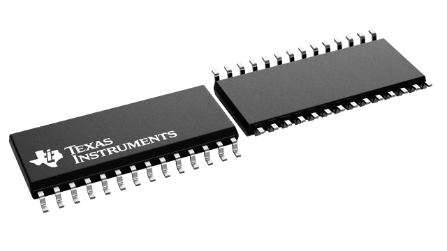
ActiveLOW-POWER LINBICMOS MULTIPLE DRIVERS AND RECEIVERS 28-SOIC 0 TO 70
Deep-Dive with AI
Search across all available documentation for this part.
SN75LBC241DWR
ActiveLOW-POWER LINBICMOS MULTIPLE DRIVERS AND RECEIVERS 28-SOIC 0 TO 70
Deep-Dive with AI
Technical Specifications
Parameters and characteristics commom to parts in this series
| Specification | SN75LBC241DWR | 75LBC241 Series |
|---|---|---|
| Data Rate | 100 Kbps | 100 Kbps |
| Duplex | Full | Full |
| Mounting Type | Surface Mount | Surface Mount |
| Number of Drivers/Receivers | 5, 4 | 4 - 5 |
| Operating Temperature [Max] | 70 ░C | 70 ░C |
| Operating Temperature [Min] | 0 °C | 0 °C |
| Package / Case | 0.295 " | 0.295 " |
| Package / Case | 28-SOIC | 28-SOIC |
| Package / Case | 7.5 mm | 7.5 mm |
| Protocol | RS232 | RS232 |
| Receiver Hysteresis | 500 mV | 500 mV |
| Supplier Device Package | 28-SOIC | 28-SOIC |
| Type | Transceiver | Transceiver |
| Voltage - Supply [Max] | 5.5 V | 5.5 V |
| Voltage - Supply [Min] | 4.5 V | 4.5 V |
Pricing
Prices provided here are for design reference only. For realtime values and availability, please visit the distributors directly
75LBC241 Series
Low-Power LinBiCMOS Multiple Drivers And Receivers
| Part | Supplier Device Package | Operating Temperature [Max] | Operating Temperature [Min] | Package / Case | Package / Case | Package / Case | Duplex | Number of Drivers/Receivers | Data Rate | Protocol | Voltage - Supply [Max] | Voltage - Supply [Min] | Type | Receiver Hysteresis | Mounting Type |
|---|---|---|---|---|---|---|---|---|---|---|---|---|---|---|---|
Texas Instruments SN75LBC241DWRThe SN75LBC241 is a low-power LinBiCMOSTMline-interface device containing four independent drivers and five receivers. It is designed as a plug-in replacement for the Maxim MAX241. The SN75LBC241 provides a capacitive-charge-pump voltage generator to produce RS-232 voltage levels from a 5-V supply. The charge-pump oscillator frequency is 20 kHz. Each receiver converts RS-232 inputs to 5-V TTL/CMOS levels. The receivers have a typical threshold of 1.2 V and a typical hysteresis of 0.5 V and can accept ±30-V inputs. Each driver converts TTL/CMOS input levels into RS-232 levels.
The SN75LBC241 includes a receiver, a 3-state control line, and a low-power shutdown control line. When the EN\ line is high, receiver outputs are placed in the high-impedance state. When EN\ is low, normal operation is enabled.
The shutdown mode reduces power dissipation to less than 5 uW, typically. In this mode, receiver outputs have high impedance, driver outputs are turned off, and the charge-pump circuit is turned off. When SHUTDOWN is high, the shutdown mode is enabled. When SHUTDOWN is low, normal operation is enabled.
This device has been designed to conform to TIA/EIA-232-F and ITU Recommendation V.28.
The SN75LBC241 has been designed using LinBiCMOS technology and cells contained in the Texas Instruments LinASICTMlibrary. Use of LinBiCMOS circuitry increases latch-up immunity in this device over an all-CMOS design.
The SN75LBC241 is characterized for operation from 0°C to 70°C.
The SN75LBC241 is a low-power LinBiCMOSTMline-interface device containing four independent drivers and five receivers. It is designed as a plug-in replacement for the Maxim MAX241. The SN75LBC241 provides a capacitive-charge-pump voltage generator to produce RS-232 voltage levels from a 5-V supply. The charge-pump oscillator frequency is 20 kHz. Each receiver converts RS-232 inputs to 5-V TTL/CMOS levels. The receivers have a typical threshold of 1.2 V and a typical hysteresis of 0.5 V and can accept ±30-V inputs. Each driver converts TTL/CMOS input levels into RS-232 levels.
The SN75LBC241 includes a receiver, a 3-state control line, and a low-power shutdown control line. When the EN\ line is high, receiver outputs are placed in the high-impedance state. When EN\ is low, normal operation is enabled.
The shutdown mode reduces power dissipation to less than 5 uW, typically. In this mode, receiver outputs have high impedance, driver outputs are turned off, and the charge-pump circuit is turned off. When SHUTDOWN is high, the shutdown mode is enabled. When SHUTDOWN is low, normal operation is enabled.
This device has been designed to conform to TIA/EIA-232-F and ITU Recommendation V.28.
The SN75LBC241 has been designed using LinBiCMOS technology and cells contained in the Texas Instruments LinASICTMlibrary. Use of LinBiCMOS circuitry increases latch-up immunity in this device over an all-CMOS design.
The SN75LBC241 is characterized for operation from 0°C to 70°C. | 28-SOIC | 70 ░C | 0 °C | 0.295 " | 28-SOIC | 7.5 mm | Full | 4, 5 | 100 Kbps | RS232 | 5.5 V | 4.5 V | Transceiver | 500 mV | Surface Mount |
Texas Instruments SN75LBC241DWThe SN75LBC241 is a low-power LinBiCMOSTMline-interface device containing four independent drivers and five receivers. It is designed as a plug-in replacement for the Maxim MAX241. The SN75LBC241 provides a capacitive-charge-pump voltage generator to produce RS-232 voltage levels from a 5-V supply. The charge-pump oscillator frequency is 20 kHz. Each receiver converts RS-232 inputs to 5-V TTL/CMOS levels. The receivers have a typical threshold of 1.2 V and a typical hysteresis of 0.5 V and can accept ±30-V inputs. Each driver converts TTL/CMOS input levels into RS-232 levels.
The SN75LBC241 includes a receiver, a 3-state control line, and a low-power shutdown control line. When the EN\ line is high, receiver outputs are placed in the high-impedance state. When EN\ is low, normal operation is enabled.
The shutdown mode reduces power dissipation to less than 5 uW, typically. In this mode, receiver outputs have high impedance, driver outputs are turned off, and the charge-pump circuit is turned off. When SHUTDOWN is high, the shutdown mode is enabled. When SHUTDOWN is low, normal operation is enabled.
This device has been designed to conform to TIA/EIA-232-F and ITU Recommendation V.28.
The SN75LBC241 has been designed using LinBiCMOS technology and cells contained in the Texas Instruments LinASICTMlibrary. Use of LinBiCMOS circuitry increases latch-up immunity in this device over an all-CMOS design.
The SN75LBC241 is characterized for operation from 0°C to 70°C.
The SN75LBC241 is a low-power LinBiCMOSTMline-interface device containing four independent drivers and five receivers. It is designed as a plug-in replacement for the Maxim MAX241. The SN75LBC241 provides a capacitive-charge-pump voltage generator to produce RS-232 voltage levels from a 5-V supply. The charge-pump oscillator frequency is 20 kHz. Each receiver converts RS-232 inputs to 5-V TTL/CMOS levels. The receivers have a typical threshold of 1.2 V and a typical hysteresis of 0.5 V and can accept ±30-V inputs. Each driver converts TTL/CMOS input levels into RS-232 levels.
The SN75LBC241 includes a receiver, a 3-state control line, and a low-power shutdown control line. When the EN\ line is high, receiver outputs are placed in the high-impedance state. When EN\ is low, normal operation is enabled.
The shutdown mode reduces power dissipation to less than 5 uW, typically. In this mode, receiver outputs have high impedance, driver outputs are turned off, and the charge-pump circuit is turned off. When SHUTDOWN is high, the shutdown mode is enabled. When SHUTDOWN is low, normal operation is enabled.
This device has been designed to conform to TIA/EIA-232-F and ITU Recommendation V.28.
The SN75LBC241 has been designed using LinBiCMOS technology and cells contained in the Texas Instruments LinASICTMlibrary. Use of LinBiCMOS circuitry increases latch-up immunity in this device over an all-CMOS design.
The SN75LBC241 is characterized for operation from 0°C to 70°C. | 28-SOIC | 70 ░C | 0 °C | 0.295 " | 28-SOIC | 7.5 mm | Full | 4, 5 | 100 Kbps | RS232 | 5.5 V | 4.5 V | Transceiver | 500 mV | Surface Mount |
Description
General part information
75LBC241 Series
The SN75LBC241 is a low-power LinBiCMOSTMline-interface device containing four independent drivers and five receivers. It is designed as a plug-in replacement for the Maxim MAX241. The SN75LBC241 provides a capacitive-charge-pump voltage generator to produce RS-232 voltage levels from a 5-V supply. The charge-pump oscillator frequency is 20 kHz. Each receiver converts RS-232 inputs to 5-V TTL/CMOS levels. The receivers have a typical threshold of 1.2 V and a typical hysteresis of 0.5 V and can accept ±30-V inputs. Each driver converts TTL/CMOS input levels into RS-232 levels.
The SN75LBC241 includes a receiver, a 3-state control line, and a low-power shutdown control line. When the EN\ line is high, receiver outputs are placed in the high-impedance state. When EN\ is low, normal operation is enabled.
The shutdown mode reduces power dissipation to less than 5 uW, typically. In this mode, receiver outputs have high impedance, driver outputs are turned off, and the charge-pump circuit is turned off. When SHUTDOWN is high, the shutdown mode is enabled. When SHUTDOWN is low, normal operation is enabled.
Documents
Technical documentation and resources