


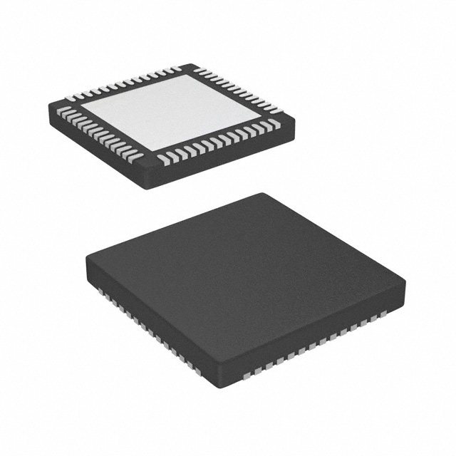
VSP5610RSHR
Active16 BIT, 35MSPS FOUR CHANNEL IMAGING ANALOG FRONT END

VSP5610RSHR
Active16 BIT, 35MSPS FOUR CHANNEL IMAGING ANALOG FRONT END
Description
General part information
VSP5610 Series
The VSP5610/11/12 are high-speed, high-performance, 16-bit analog-to-digital-converters (ADCs) that have four independent sampling circuit channels for multi-output charge-coupled device (CCD) and complementary metal oxide semiconductor (CMOS) line sensors. Pixel data from the sensor are sampled by the sample/hold (SH) or correlated double sampler (CDS) circuit, and are then converted to digital data by an ADC. Data output is selectable in low-voltage differential signaling (LVDS) or CMOS modes.
The VSP5610/11/12 include a programmable gain to support the pixel level inflection caused by luminance. The integrated digital-to-analog-converter (DAC) can be used to adjust the offset level for the analog input signal. Furthermore, the timing generator (TG) is integrated in these devices for the control of sensor operation.
The VSP5610/11/12 use 1.65 V to 1.95 V for the core voltage and 3.0 V to 3.6 V for I/Os. The core voltage is supplied by a built-in low-dropout regulator (LDO).
Technical Specifications
Parameters and characteristics for this part
| Specification | VSP5610RSHR |
|---|---|
| Mounting Type | Surface Mount |
| Number of Bits | 16 bits |
| Number of Channels | 4 |
| Package / Case | 56-VFQFN Exposed Pad |
| Package Length | 7 mm |
| Package Name | 56-VQFN |
| Package Width | 7 mm |
| Power (Watts) | 426 mW |
| Voltage - Supply, Analog (Max) | 3.6 V |
| Voltage - Supply, Analog (Min) | 3 V |
| Voltage - Supply, Digital (Max) | 3.6 V |
| Voltage - Supply, Digital (Min) | 3 V |
Pricing
Prices provided here are for design reference only. For realtime values and availability, please visit the distributors directly
Sign in to see pricing
Create a free account to access distributor pricing data.
CAD
3D models and CAD resources for this part
Documents
Technical documentation and resources