ADC08B200CIVS/NOPB
Active8-BIT, 200-MSPS, ANALOG-TO-DIGITAL CONVERTER (ADC) WITH 1K BUFFER
Deep-Dive with AI
Search across all available documentation for this part.
ADC08B200CIVS/NOPB
Active8-BIT, 200-MSPS, ANALOG-TO-DIGITAL CONVERTER (ADC) WITH 1K BUFFER
Technical Specifications
Parameters and characteristics commom to parts in this series
| Specification | ADC08B200CIVS/NOPB | ADC08B200 Series |
|---|---|---|
| Configuration | ADC | ADC |
| Data Interface | Parallel | Parallel |
| Grade | - | Automotive |
| Input Type | Single Ended | Single Ended |
| Mounting Type | Surface Mount | Surface Mount |
| Number of A/D Converters | 1 | 1 |
| Number of Bits | 8 | 8 |
| Number of Inputs | 1 | 1 |
| Operating Temperature [Max] | 105 ░C | 105 ░C |
| Operating Temperature [Min] | -40 °C | -40 °C |
| Package / Case | 48-TQFP | 48-TQFP |
| Qualification | - | AEC-Q100 |
| Reference Type | External | External |
| Sampling Rate (Per Second) | 200 M | 200 M |
| Supplier Device Package | 48-TQFP (7x7) | 48-TQFP (7x7) |
| Voltage - Supply, Analog [Max] | 3.6 V | 3.6 V |
| Voltage - Supply, Analog [Min] | 3 V | 3 V |
| Voltage - Supply, Digital [Max] | 3.6 V | 3.6 V |
| Voltage - Supply, Digital [Min] | 2.7 V | 2.7 V |
Pricing
Prices provided here are for design reference only. For realtime values and availability, please visit the distributors directly
ADC08B200 Series
8-Bit, 200-MSPS, Analog-to-Digital Converter (ADC) with 1K Buffer
| Part | Operating Temperature [Min] | Operating Temperature [Max] | Supplier Device Package | Number of Bits | Number of A/D Converters | Input Type | Package / Case | Mounting Type | Data Interface | Voltage - Supply, Analog [Max] | Voltage - Supply, Analog [Min] | Voltage - Supply, Digital [Min] | Voltage - Supply, Digital [Max] | Sampling Rate (Per Second) | Configuration | Number of Inputs | Reference Type | Qualification | Grade |
|---|---|---|---|---|---|---|---|---|---|---|---|---|---|---|---|---|---|---|---|
Texas Instruments ADC08B200CIVS/NOPBThe ADC08B200 is a high speed analog-to-digital converter (ADC) with an integrated capture buffer. The 8-bit, 200 MSPS A/D core is based upon the proven ADC08200 with integrated track-and-hold and is optimized for low power consumption. This device contains a selectable size capture buffer of up to 1,024 bytes that allows fast capture of an input signal with a slower readout rate. An on-chip clock PLL circuit provides the option of on-chip clock rate multiplication to provide the high speed sampling clock.
The ADC08B200 is resistant to latch-up and the outputs are short-circuit proof. The top and bottom of the ADC08B200's reference ladder are available for connections, enabling a wide range of input possibilities. The digital outputs are TTL/CMOS compatible with a separate output power supply pin to support interfacing with 2.7V to 3.3V logic. The digital inputs and outputs are low voltage TTL/CMOS compatible and the output data format is straight binary.
The ADC08B200Q runs on an Automotive Grade Flow and is AEC-Q100 Grade 2 Qualified.
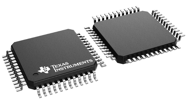
The ADC08B200 is offered in a 48-pin plastic package (TQFP) and is specified over the extended industrial temperature range of −40°C to +105°C. An evaluation board is available to assist in the easy evaluation of the ADC08B200.
The ADC08B200 is a high speed analog-to-digital converter (ADC) with an integrated capture buffer. The 8-bit, 200 MSPS A/D core is based upon the proven ADC08200 with integrated track-and-hold and is optimized for low power consumption. This device contains a selectable size capture buffer of up to 1,024 bytes that allows fast capture of an input signal with a slower readout rate. An on-chip clock PLL circuit provides the option of on-chip clock rate multiplication to provide the high speed sampling clock.
The ADC08B200 is resistant to latch-up and the outputs are short-circuit proof. The top and bottom of the ADC08B200's reference ladder are available for connections, enabling a wide range of input possibilities. The digital outputs are TTL/CMOS compatible with a separate output power supply pin to support interfacing with 2.7V to 3.3V logic. The digital inputs and outputs are low voltage TTL/CMOS compatible and the output data format is straight binary.
The ADC08B200Q runs on an Automotive Grade Flow and is AEC-Q100 Grade 2 Qualified.
The ADC08B200 is offered in a 48-pin plastic package (TQFP) and is specified over the extended industrial temperature range of −40°C to +105°C. An evaluation board is available to assist in the easy evaluation of the ADC08B200. | -40 °C | 105 ░C | 48-TQFP (7x7) | 8 | 1 | Single Ended | 48-TQFP | Surface Mount | Parallel | 3.6 V | 3 V | 2.7 V | 3.6 V | 200 M | ADC | 1 | External | ||
Texas Instruments ADC08B200QCIVS/NOPBThe ADC08B200 is a high speed analog-to-digital converter (ADC) with an integrated capture buffer. The 8-bit, 200 MSPS A/D core is based upon the proven ADC08200 with integrated track-and-hold and is optimized for low power consumption. This device contains a selectable size capture buffer of up to 1,024 bytes that allows fast capture of an input signal with a slower readout rate. An on-chip clock PLL circuit provides the option of on-chip clock rate multiplication to provide the high speed sampling clock.
The ADC08B200 is resistant to latch-up and the outputs are short-circuit proof. The top and bottom of the ADC08B200's reference ladder are available for connections, enabling a wide range of input possibilities. The digital outputs are TTL/CMOS compatible with a separate output power supply pin to support interfacing with 2.7V to 3.3V logic. The digital inputs and outputs are low voltage TTL/CMOS compatible and the output data format is straight binary.
The ADC08B200Q runs on an Automotive Grade Flow and is AEC-Q100 Grade 2 Qualified.
The ADC08B200 is offered in a 48-pin plastic package (TQFP) and is specified over the extended industrial temperature range of −40°C to +105°C. An evaluation board is available to assist in the easy evaluation of the ADC08B200.
The ADC08B200 is a high speed analog-to-digital converter (ADC) with an integrated capture buffer. The 8-bit, 200 MSPS A/D core is based upon the proven ADC08200 with integrated track-and-hold and is optimized for low power consumption. This device contains a selectable size capture buffer of up to 1,024 bytes that allows fast capture of an input signal with a slower readout rate. An on-chip clock PLL circuit provides the option of on-chip clock rate multiplication to provide the high speed sampling clock.
The ADC08B200 is resistant to latch-up and the outputs are short-circuit proof. The top and bottom of the ADC08B200's reference ladder are available for connections, enabling a wide range of input possibilities. The digital outputs are TTL/CMOS compatible with a separate output power supply pin to support interfacing with 2.7V to 3.3V logic. The digital inputs and outputs are low voltage TTL/CMOS compatible and the output data format is straight binary.
The ADC08B200Q runs on an Automotive Grade Flow and is AEC-Q100 Grade 2 Qualified.
The ADC08B200 is offered in a 48-pin plastic package (TQFP) and is specified over the extended industrial temperature range of −40°C to +105°C. An evaluation board is available to assist in the easy evaluation of the ADC08B200. | -40 °C | 105 ░C | 48-TQFP (7x7) | 8 | 1 | Single Ended | 48-TQFP | Surface Mount | Parallel | 3.6 V | 3 V | 2.7 V | 3.6 V | 200 M | ADC | 1 | External | AEC-Q100 | Automotive |
Description
General part information
ADC08B200 Series
The ADC08B200 is a high speed analog-to-digital converter (ADC) with an integrated capture buffer. The 8-bit, 200 MSPS A/D core is based upon the proven ADC08200 with integrated track-and-hold and is optimized for low power consumption. This device contains a selectable size capture buffer of up to 1,024 bytes that allows fast capture of an input signal with a slower readout rate. An on-chip clock PLL circuit provides the option of on-chip clock rate multiplication to provide the high speed sampling clock.
The ADC08B200 is resistant to latch-up and the outputs are short-circuit proof. The top and bottom of the ADC08B200's reference ladder are available for connections, enabling a wide range of input possibilities. The digital outputs are TTL/CMOS compatible with a separate output power supply pin to support interfacing with 2.7V to 3.3V logic. The digital inputs and outputs are low voltage TTL/CMOS compatible and the output data format is straight binary.
The ADC08B200Q runs on an Automotive Grade Flow and is AEC-Q100 Grade 2 Qualified.
Documents
Technical documentation and resources