DS90LV049HMTX/NOPB
ActiveHIGH TEMPERATURE 3-V LVDS DUAL LINE DRIVER AND RECEIVER PAIR
DS90LV049HMTX/NOPB
ActiveHIGH TEMPERATURE 3-V LVDS DUAL LINE DRIVER AND RECEIVER PAIR
Description
General part information
DS90LV049 Series
The DS90LV049 is a dual CMOS flow-through differential line driver-receiver pair designed for applications requiring ultra low power dissipation, exceptional noise immunity, and high data throughput. The device is designed to support data rates in excess of 400 Mbps utilizing Low Voltage Differential Signaling (LVDS) technology.
The DS90LV049 drivers accept LVTTL/LVCMOS signals and translate them to LVDS signals. On the other hand, the receivers accept LVDS signals and translate them to 3 V CMOS signals. The LVDS input buffers have internal failsafe biasing that places the outputs to a known H (high) state for floating receiver inputs. In addition, the DS90LV049 supports a TRI-STATE function for a low idle power state when the device is not in use.
The EN andENinputs are ANDed together and control the TRI-STATE outputs. The enables are common to all four gates.
Technical Specifications
Parameters and characteristics for this part
| Specification | DS90LV049HMTX/NOPB |
|---|---|
| Data Rate | 400 Mbps |
| Duplex | Full |
| Mounting Type | Surface Mount |
| Number of Drivers | 2 |
| Number of Receivers | 2 |
| Operating Temperature (Max) | 125 °C |
| Operating Temperature (Min) | -40 °C |
| Package Length | 0.173 in |
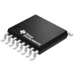
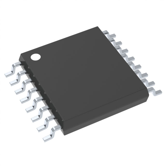
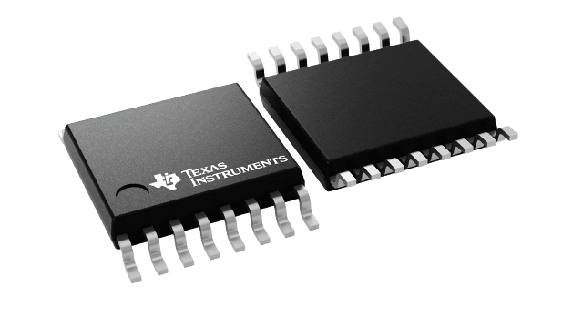
| Package Name | 16-TSSOP |
| Package Width | 4.4 mm |
| Protocol | LVDS |
| Type | Transceiver |
| Voltage - Supply (Maximum) | 3.6 V |
| Voltage - Supply (Minimum) | 3 V |
Pricing
Prices provided here are for design reference only. For realtime values and availability, please visit the distributors directly
Sign in to see pricing
Create a free account to access distributor pricing data.
CAD
3D models and CAD resources for this part
Documents
Technical documentation and resources