DAC5675AHFG/EM
ActiveQMLV, 150-KRAD, CERAMIC, 14-BIT, SINGLE-CHANNEL, 400-MSPS DAC
Deep-Dive with AI
Search across all available documentation for this part.
DAC5675AHFG/EM
ActiveQMLV, 150-KRAD, CERAMIC, 14-BIT, SINGLE-CHANNEL, 400-MSPS DAC
Technical Specifications
Parameters and characteristics for this part
| Specification | DAC5675AHFG/EM |
|---|---|
| Architecture | Current Source |
| Data Interface | LVDS - Parallel |
| Differential Output | True |
| INL/DNL (LSB) [Max] | 1.5 LSB |
| INL/DNL (LSB) [Min] | -1.5 LSB |
| Mounting Type | Surface Mount |
| Number of Bits | 14 |
| Operating Temperature [Max] | 85 °C |
| Operating Temperature [Min] | -40 °C |
| Output Type | Current - Unbuffered |
| Package / Case | 52-CFlatPack |
| Reference Type | Internal, External |
| Settling Time | 12 ns |
| Supplier Device Package | 52-CFP |
| Voltage - Supply, Analog [Max] | 3.6 V |
| Voltage - Supply, Analog [Min] | 3.15 V |
| Voltage - Supply, Digital [Max] | 3.6 V |
| Voltage - Supply, Digital [Min] | 3.15 V |
Pricing
Prices provided here are for design reference only. For realtime values and availability, please visit the distributors directly
DAC5675A-SP Series
QMLV, 150-krad, ceramic, 14-bit, single-channel, 400-MSPS DAC
| Part | Supplier Device Package | Differential Output | Voltage - Supply, Digital [Max] | Voltage - Supply, Digital [Min] | Architecture | Settling Time | Mounting Type | Data Interface | Number of Bits | Reference Type | Voltage - Supply, Analog [Min] | Voltage - Supply, Analog [Max] | Operating Temperature [Min] | Operating Temperature [Max] | INL/DNL (LSB) [Max] | INL/DNL (LSB) [Min] | Output Type | Package / Case |
|---|---|---|---|---|---|---|---|---|---|---|---|---|---|---|---|---|---|---|
Texas Instruments DAC5675AHFG/EMThe DAC5675A-SP is a radiation-tolerant, 14-bit resolution high-speed digital-to-analog converter (DAC) primarily suited for space satellite applications. The DAC5675A-SP is designed for high-speed digital data transmission in wired and wireless communication systems, high-frequency direct digital synthesis (DDS), and waveform reconstruction in test and measurement applications. The DAC5675A-SP has excellent SFDR at high intermediate frequencies, which makes it well suited for multicarrier transmission in TDMA and CDMA based cellular base transceiver stations (BTSs).
The DAC5675A-SP operates from a single supply voltage of 3.3 V. Power dissipation is 660 mW at ƒCLK= 400 MSPS, ƒOUT= 70 MHz. The DAC5675A-SP provides a nominal full-scale differential current output of 20 mA, supporting both single-ended and differential applications. The output current can be directly fed to the load with no additional external output buffer required. The output is referred to the analog supply voltage AVDD.
The DAC5675A-SP includes a low-voltage differential signaling (LVDS) interface for high-speed digital data input. LVDS features a low differential voltage swing with a low constant power consumption across frequency, allowing for high-speed data transmission with low noise levels (low electromagnetic interference (EMI)).
LVDS is typically implemented in low-voltage digital CMOS processes, making it the ideal technology for high-speed interfacing between the DAC5675A-SP and high-speed low-voltage CMOS ASICs or FPGAs.
The DAC5675A-SP current-source-array architecture supports update rates of up to 400 MSPS. On-chip edge-triggered input latches provide for minimum setup and hold times, thereby relaxing interface timing.
The DAC5675A-SP is specifically designed for a differential transformer-coupled output with a 50-Ω doubly-terminated load. With the 20-mA full-scale output current, both a 4:1 impedance ratio (resulting in an output power of 4 dBm) and 1:1 impedance ratio transformer (–2 dBm) is supported. The last configuration is preferred for optimum performance at high output frequencies and update rates. The outputs are terminated to AVDD and have voltage compliance ranges from AVDD– 1 to AVDD+ 0.3 V.
An accurate on-chip 1.2-V temperature-compensated bandgap reference and control amplifier allows the user to adjust this output current from 20 to 2 mA. This provides 20-dB gain range control capabilities. Alternatively, an external reference voltage may be applied. The DAC5675A-SP features a SLEEP mode, which reduces the standby power to approximately 18 mW.
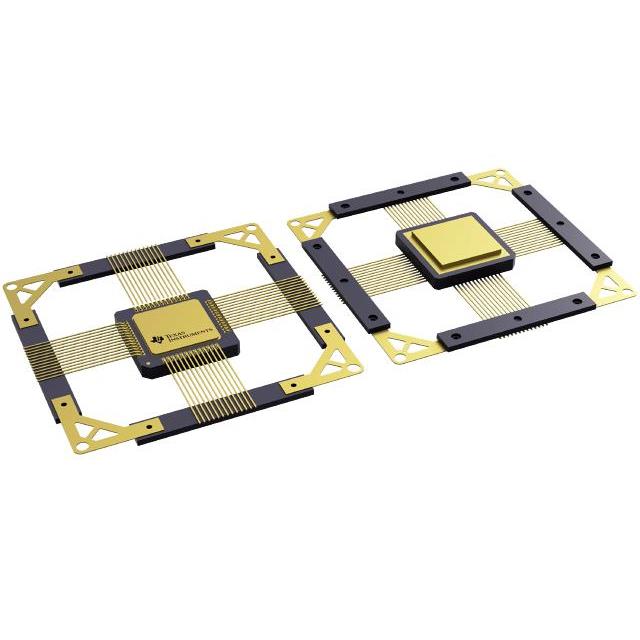
The DAC5675A-SP is available in a 52-pin ceramic nonconductive tie-bar package (HFG). The device is specified for operation over the military temperature range of –55°C to 125°C and W temperature range of –55°C to 115°C.
The DAC5675A-SP is a radiation-tolerant, 14-bit resolution high-speed digital-to-analog converter (DAC) primarily suited for space satellite applications. The DAC5675A-SP is designed for high-speed digital data transmission in wired and wireless communication systems, high-frequency direct digital synthesis (DDS), and waveform reconstruction in test and measurement applications. The DAC5675A-SP has excellent SFDR at high intermediate frequencies, which makes it well suited for multicarrier transmission in TDMA and CDMA based cellular base transceiver stations (BTSs).
The DAC5675A-SP operates from a single supply voltage of 3.3 V. Power dissipation is 660 mW at ƒCLK= 400 MSPS, ƒOUT= 70 MHz. The DAC5675A-SP provides a nominal full-scale differential current output of 20 mA, supporting both single-ended and differential applications. The output current can be directly fed to the load with no additional external output buffer required. The output is referred to the analog supply voltage AVDD.
The DAC5675A-SP includes a low-voltage differential signaling (LVDS) interface for high-speed digital data input. LVDS features a low differential voltage swing with a low constant power consumption across frequency, allowing for high-speed data transmission with low noise levels (low electromagnetic interference (EMI)).
LVDS is typically implemented in low-voltage digital CMOS processes, making it the ideal technology for high-speed interfacing between the DAC5675A-SP and high-speed low-voltage CMOS ASICs or FPGAs.
The DAC5675A-SP current-source-array architecture supports update rates of up to 400 MSPS. On-chip edge-triggered input latches provide for minimum setup and hold times, thereby relaxing interface timing.
The DAC5675A-SP is specifically designed for a differential transformer-coupled output with a 50-Ω doubly-terminated load. With the 20-mA full-scale output current, both a 4:1 impedance ratio (resulting in an output power of 4 dBm) and 1:1 impedance ratio transformer (–2 dBm) is supported. The last configuration is preferred for optimum performance at high output frequencies and update rates. The outputs are terminated to AVDD and have voltage compliance ranges from AVDD– 1 to AVDD+ 0.3 V.
An accurate on-chip 1.2-V temperature-compensated bandgap reference and control amplifier allows the user to adjust this output current from 20 to 2 mA. This provides 20-dB gain range control capabilities. Alternatively, an external reference voltage may be applied. The DAC5675A-SP features a SLEEP mode, which reduces the standby power to approximately 18 mW.
The DAC5675A-SP is available in a 52-pin ceramic nonconductive tie-bar package (HFG). The device is specified for operation over the military temperature range of –55°C to 125°C and W temperature range of –55°C to 115°C. | 52-CFP | 3.6 V | 3.15 V | Current Source | 12 ns | Surface Mount | LVDS - Parallel | 14 | External, Internal | 3.15 V | 3.6 V | -40 °C | 85 °C | 1.5 LSB | -1.5 LSB | Current - Unbuffered | 52-CFlatPack |
Description
General part information
DAC5675A-SP Series
The DAC5675A-SP is a radiation-tolerant, 14-bit resolution high-speed digital-to-analog converter (DAC) primarily suited for space satellite applications. The DAC5675A-SP is designed for high-speed digital data transmission in wired and wireless communication systems, high-frequency direct digital synthesis (DDS), and waveform reconstruction in test and measurement applications. The DAC5675A-SP has excellent SFDR at high intermediate frequencies, which makes it well suited for multicarrier transmission in TDMA and CDMA based cellular base transceiver stations (BTSs).
The DAC5675A-SP operates from a single supply voltage of 3.3 V. Power dissipation is 660 mW at ƒCLK= 400 MSPS, ƒOUT= 70 MHz. The DAC5675A-SP provides a nominal full-scale differential current output of 20 mA, supporting both single-ended and differential applications. The output current can be directly fed to the load with no additional external output buffer required. The output is referred to the analog supply voltage AVDD.
The DAC5675A-SP includes a low-voltage differential signaling (LVDS) interface for high-speed digital data input. LVDS features a low differential voltage swing with a low constant power consumption across frequency, allowing for high-speed data transmission with low noise levels (low electromagnetic interference (EMI)).
Documents
Technical documentation and resources