


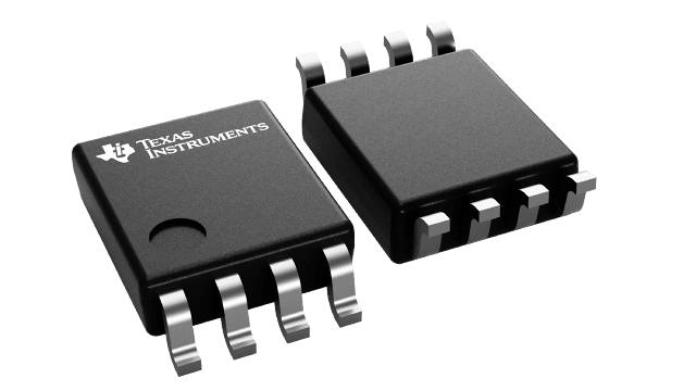
SN74LVC1G99QDCURQ1
ActiveAUTOMOTIVE CATALOG ULTRA-CONFIGURABLE MULTI-FUNCTION GATE WITH 3-STATE OUTPUTS

SN74LVC1G99QDCURQ1
ActiveAUTOMOTIVE CATALOG ULTRA-CONFIGURABLE MULTI-FUNCTION GATE WITH 3-STATE OUTPUTS
Description
General part information
SN74LVC1G99 Series
The SN74LVC1G99-Q1 is operational from 1.65 V to 5.5 V.
The SN74LVC1G99-Q1 features configurable multiple functions with a 3-state output. The output is disabled when the output-enable (OE) input is high. WhenOEis low, the output state is determined by 16 patterns of 4-bit input. The user can choose logic functions, such as MUX, AND, OR, NAND, NOR, XOR, XNOR, inverter, and buffer. All inputs can be connected to VCCor GND.
This device functions as an independent inverter, but because of Schmitt action, it has different input threshold levels for positive-going (VT+) and negative-going (VT–) signals.
Technical Specifications
Parameters and characteristics for this part
| Specification | SN74LVC1G99QDCURQ1 |
|---|---|
| Current - Output High | 32 mA |
| Current - Output Low | 32 mA |
| Grade | Automotive |
| Logic Type | Configurable Multiple Function |
| Mounting Type | Surface Mount |
| Number of Circuits | 1 |
| Number of Inputs | 4 |
| Operating Temperature (Max) | 125 °C |
| Operating Temperature (Min) | -40 °C |
| Output Type | Tri-State |
| Package Length | 0.091 in |
| Package Name | 8-VSSOP, 8-VFSOP |
| Package Width | 2.3 mm |
| Qualification | AEC-Q100 |
| Schmitt Trigger Input | Yes, No |
| Voltage - Supply (Maximum) | 5.5 V |
| Voltage - Supply (Minimum) | 1.65 V |
Pricing
Prices provided here are for design reference only. For realtime values and availability, please visit the distributors directly
Sign in to see pricing
Create a free account to access distributor pricing data.
CAD
3D models and CAD resources for this part
Documents
Technical documentation and resources