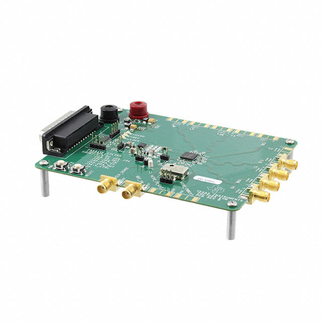
CDC7005ZVAT
ActiveHIGH PERFORMANCE, LOW PHASE NOISE, LOW SKEW CLOCK SYNCHRONIZER THAT SYNCHRONIZES REF CLOCK TO VCXO
CDC7005ZVAT
ActiveHIGH PERFORMANCE, LOW PHASE NOISE, LOW SKEW CLOCK SYNCHRONIZER THAT SYNCHRONIZES REF CLOCK TO VCXO
Description
General part information
CDC7005 Series
The CDC7005 is a high-performance, low-phase noise, and low-skew clock synchronizer and jitter cleaner that synchronizes the voltage controlled crystal oscillator (VCXO) frequency to the reference clock. The programmable predividers M and N give a high flexibility to the frequency ratio of the reference clock to VCXO: VCXO_IN/REF_IN = (NxP)/M. The VCXO_IN clock operates up to 800 MHz. Through the selection of external VCXO and loop filter components, the PLL loop bandwidth and damping factor can be adjusted to meet different system requirements. Each of the five differential LVPECL outputs is programmable by the serial peripheral interface (SPI). The SPI allows individual control of frequency and enable/disable state of each output. The device operates in 3.3-V environment. The built-in latches ensure that all outputs are synchronized.
The CDC7005 is characterized for operation from –40°C to 85°C.
The CDC7005 is a high-performance, low-phase noise, and low-skew clock synchronizer and jitter cleaner that synchronizes the voltage controlled crystal oscillator (VCXO) frequency to the reference clock. The programmable predividers M and N give a high flexibility to the frequency ratio of the reference clock to VCXO: VCXO_IN/REF_IN = (NxP)/M. The VCXO_IN clock operates up to 800 MHz. Through the selection of external VCXO and loop filter components, the PLL loop bandwidth and damping factor can be adjusted to meet different system requirements. Each of the five differential LVPECL outputs is programmable by the serial peripheral interface (SPI). The SPI allows individual control of frequency and enable/disable state of each output. The device operates in 3.3-V environment. The built-in latches ensure that all outputs are synchronized.
Technical Specifications
Parameters and characteristics for this part
| Specification | CDC7005ZVAT |
|---|---|
| Differential Input | Yes |
| Differential Output | Yes |
| Divider | Yes |
| Frequency - Max | 800 MHz |
| Input | LVCMOS, LVPECL |
| Input Ratio | 2 |
| Mounting Type | Surface Mount |
| Multiplier | Yes |
| Number of Circuits | 1 |
| Operating Temperature (Max) | 85 °C |
| Operating Temperature (Min) | -40 °C |
| Output | LVPECL |
| Output Ratio | 5 |
| Package / Case | 64-LFBGA |
| Package Length | 8 mm |
| Package Name | 64-BGA |
| Package Width | 8 mm |
| PLL | No |
| Type | Clock Synchronizer and Jitter Cleaner |
| Voltage - Supply (Maximum) | 3.6 V |
| Voltage - Supply (Minimum) | 3 V |
Pricing
Prices provided here are for design reference only. For realtime values and availability, please visit the distributors directly
Sign in to see pricing
Create a free account to access distributor pricing data.
CAD
3D models and CAD resources for this part
Documents
Technical documentation and resources