TPS71918-12DRVT
Active200-MA, LOW-IQ, HIGH-PSRR, DUAL-CHANNEL LOW-DROPOUT VOLTAGE REGULATOR WITH ACTIVE PULLDOWN
TPS71918-12DRVT
Active200-MA, LOW-IQ, HIGH-PSRR, DUAL-CHANNEL LOW-DROPOUT VOLTAGE REGULATOR WITH ACTIVE PULLDOWN
Description
General part information
TPS719 Series
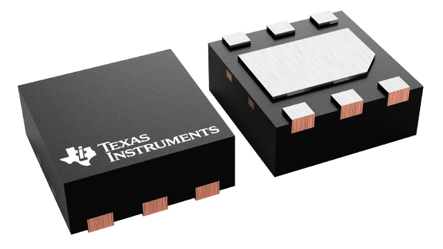
The TPS718xx and TPS719xx families of low-dropout (LDO) regulators offer a high power-supply rejection ratio (PSRR), low noise, fast start-up, and excellent line and load transient responses while consuming a very low 90µA (typical) at no load ground current with both LDOs enabled. The TPS719xx also provides an active pulldown circuit to quickly discharge output loads. The TPS718xx and TPS719xx are stable with ceramic capacitors and use an advanced BiCMOS fabrication process to yield a typical dropout voltage of 230mV at 200mA output loads. The TPS718xx and TPS719xx also use a precision voltage reference and feedback loop to achieve 3% overall accuracy over all load, line, process, and temperature variations. Both families of devices are fully specified from TJ= -40°C to +125°C and are offered in 2mm × 2mm SON-6 and 6-ball Wafer Chip-Scale (WCSP) packages that are ideal for applications such as mobile handsets and WLAN that require good thermal dissipation while maintaining a very small footprint.
The TPS718xx and TPS719xx families of low-dropout (LDO) regulators offer a high power-supply rejection ratio (PSRR), low noise, fast start-up, and excellent line and load transient responses while consuming a very low 90µA (typical) at no load ground current with both LDOs enabled. The TPS719xx also provides an active pulldown circuit to quickly discharge output loads. The TPS718xx and TPS719xx are stable with ceramic capacitors and use an advanced BiCMOS fabrication process to yield a typical dropout voltage of 230mV at 200mA output loads. The TPS718xx and TPS719xx also use a precision voltage reference and feedback loop to achieve 3% overall accuracy over all load, line, process, and temperature variations. Both families of devices are fully specified from TJ= -40°C to +125°C and are offered in 2mm × 2mm SON-6 and 6-ball Wafer Chip-Scale (WCSP) packages that are ideal for applications such as mobile handsets and WLAN that require good thermal dissipation while maintaining a very small footprint.
Technical Specifications
Parameters and characteristics for this part
| Specification | TPS71918-12DRVT |
|---|---|
| Control Features | Enable |
| Current - Output | 200 mA |
| Current - Quiescent (Iq) | 160 µA |
| Current - Supply (Max) | 250 µA |
| Mounting Type | Surface Mount |
| Number of Regulators | 2 |
| Operating Temperature (Max) | 125 °C |
| Operating Temperature (Min) | -40 °C |
| Output Configuration | Positive |
| Output Type | Fixed |
| Package / Case | 6-WDFN Exposed Pad |
| Package Length | 2 mm |
| Package Name | 6-WSON |
| Package Width | 2 mm |
| Protection Features | Over Temperature, Under Voltage Lockout (UVLO), Over Current |
| PSRR (Maximum) | 63 dB |
| PSRR (Minimum) | 44 dB |
| Voltage - Input (Max) | 6.5 V |
| Voltage - Output (Fixed) | 1.2 V |
| Voltage - Output (Min) | 1.8 V |
Pricing
Prices provided here are for design reference only. For realtime values and availability, please visit the distributors directly
Sign in to see pricing
Create a free account to access distributor pricing data.
CAD
3D models and CAD resources for this part