LMK1C1102PWR
Active2-CHANNEL OUTPUT LVCMOS 1.8-V BUFFER
LMK1C1102PWR
Active2-CHANNEL OUTPUT LVCMOS 1.8-V BUFFER
Description
General part information
LMK1C1102 Series
The LMK1C110x is a modular, high-performance, low-skew, general-purpose clock buffer family from Texas Instruments. The entire family is designed with a modular approach in mind. Three different fan-out variations, 1:2, 1:3, 1:4, are available.
All of the devices within this family are pin-compatible to each other and backwards compatible to the CDCLVC110x family for easy handling.
All family members share the same high performing characteristics such as low additive jitter, low skew, and wide operating temperature range.
Technical Specifications
Parameters and characteristics for this part
| Specification | LMK1C1102PWR |
|---|---|
| Differential Input | No |
| Differential Output | No |
| Frequency - Max | 250 MHz |
| Input | LVCMOS |
| Input Ratio | 1 |
| Mounting Type | Surface Mount |
| Number of Circuits | 1 |
| Operating Temperature (Max) | 125 °C |
| Operating Temperature (Min) | -40 °C |
| Output | LVCMOS |
| Output Ratio | 2 |
| Package Length | 0.173 in |
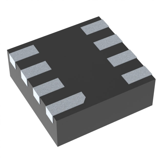
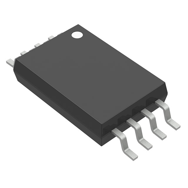
| Package Name | 8-TSSOP |
| Package Width | 4.4 mm |
| Type | Clock Buffer |
| Voltage - Supply (Range 1 Maximum) | 1.89 V |
| Voltage - Supply (Range 1 Minimum) | 1.71 V |
| Voltage - Supply (Range 2 Maximum) | 2.625 V |
| Voltage - Supply (Range 2 Minimum) | 2.375 V |
| Voltage - Supply (Range 3 Maximum) | 3.465 V |
| Voltage - Supply (Range 3 Minimum) | 3.135 V |
Pricing
Prices provided here are for design reference only. For realtime values and availability, please visit the distributors directly
Sign in to see pricing
Create a free account to access distributor pricing data.
CAD
3D models and CAD resources for this part