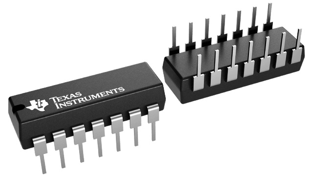
CD74HCT107E
ActiveHIGH SPEED CMOS LOGIC DUAL NEGATIVE-EDGE-TRIGGERED J-K FLIP-FLOPS WITH RESET
Deep-Dive with AI
Search across all available documentation for this part.

CD74HCT107E
ActiveHIGH SPEED CMOS LOGIC DUAL NEGATIVE-EDGE-TRIGGERED J-K FLIP-FLOPS WITH RESET
Deep-Dive with AI
Technical Specifications
Parameters and characteristics for this part
| Specification | CD74HCT107E |
|---|---|
| Clock Frequency | 56 MHz |
| Current - Output High, Low | 4 mA, 4 mA |
| Current - Quiescent (Iq) | 4 çA |
| Function | Reset |
| Input Capacitance | 10 pF |
| Max Propagation Delay @ V, Max CL | 43 ns |
| Mounting Type | Through Hole |
| Number of Bits per Element | 1 |
| Number of Elements [custom] | 2 |
| Operating Temperature [Max] | 125 °C |
| Operating Temperature [Min] | -55 C |
| Output Type | Complementary |
| Package / Case | 14-DIP |
| Package / Case | 7.62 mm |
| Package / Case | 0.3 in |
| Trigger Type | Negative Edge |
| Type | JK Type |
| Voltage - Supply [Max] | 5.5 V |
| Voltage - Supply [Min] | 4.5 V |
Pricing
Prices provided here are for design reference only. For realtime values and availability, please visit the distributors directly
CD74HCT107 Series
High Speed CMOS Logic Dual Negative-Edge-Triggered J-K Flip-Flops with Reset
| Part | Number of Elements [custom] | Number of Bits per Element | Package / Case | Package / Case | Package / Case | Output Type | Function | Current - Output High, Low | Type | Input Capacitance | Voltage - Supply [Max] | Voltage - Supply [Min] | Max Propagation Delay @ V, Max CL | Trigger Type | Clock Frequency | Mounting Type | Current - Quiescent (Iq) | Operating Temperature [Min] | Operating Temperature [Max] |
|---|---|---|---|---|---|---|---|---|---|---|---|---|---|---|---|---|---|---|---|
Texas Instruments CD74HCT107EThe ’HC107 and ’HCT107 utilize silicon gate CMOS technology to achieve operating speeds equivalent to LSTTL parts. They exhibit the low power consumption of standard CMOS integrated circuits, together with the ability to drive 10 LSTTL loads.
These flip-flops have independent J, K, Reset and Clock inputs and Q and Q\ outputs. They change state on the negative-going transition of the clock pulse. Reset is accomplished asynchronously by a low level input.
This device is functionally identical to the HC/HCT73 but differs in terminal assignment and in some parametric limits.
The HCT logic family is functionally as well as pin compatible with the standard LS family.
The ’HC107 and ’HCT107 utilize silicon gate CMOS technology to achieve operating speeds equivalent to LSTTL parts. They exhibit the low power consumption of standard CMOS integrated circuits, together with the ability to drive 10 LSTTL loads.
These flip-flops have independent J, K, Reset and Clock inputs and Q and Q\ outputs. They change state on the negative-going transition of the clock pulse. Reset is accomplished asynchronously by a low level input.
This device is functionally identical to the HC/HCT73 but differs in terminal assignment and in some parametric limits.
The HCT logic family is functionally as well as pin compatible with the standard LS family. | 2 | 1 | 14-DIP | 7.62 mm | 0.3 in | Complementary | Reset | 4 mA, 4 mA | JK Type | 10 pF | 5.5 V | 4.5 V | 43 ns | Negative Edge | 56 MHz | Through Hole | 4 çA | -55 C | 125 °C |
Description
General part information
CD74HCT107 Series
The ’HC107 and ’HCT107 utilize silicon gate CMOS technology to achieve operating speeds equivalent to LSTTL parts. They exhibit the low power consumption of standard CMOS integrated circuits, together with the ability to drive 10 LSTTL loads.
These flip-flops have independent J, K, Reset and Clock inputs and Q and Q\ outputs. They change state on the negative-going transition of the clock pulse. Reset is accomplished asynchronously by a low level input.
This device is functionally identical to the HC/HCT73 but differs in terminal assignment and in some parametric limits.
Documents
Technical documentation and resources


