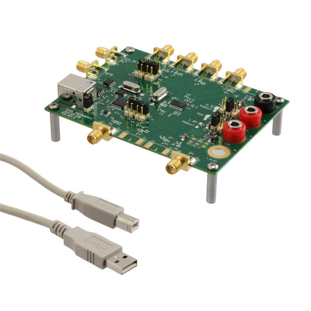
CDCE949PW
ActivePROGRAMMABLE 4-PLL VCXO CLOCK SYNTHESIZER WITH 2.5-V OR 3.3-V LVCMOS OUTPUTS
CDCE949PW
ActivePROGRAMMABLE 4-PLL VCXO CLOCK SYNTHESIZER WITH 2.5-V OR 3.3-V LVCMOS OUTPUTS
Description
General part information
CDCE949 Series
The CDCE949 is a modular PLL-based low-cost high-performance programmable clock synthesizer, multiplier, and divider. It generates up to 9 output clocks from a single input frequency. Each output can be programmed in-system for any clock frequency up to 230 MHz, using up to four independent configurable PLLs.
The CDCE949 has separate output supply pins, VDDOUT, of 2.5 V to 3.3 V.
The input accepts an external crystal or LVCMOS clock signal. If an external crystal is used, an on-chip load capacitor is adequate for most applications. The value of the load capacitor is programmable from 0 to 20 pF. Additionally, an on-chip VCXO is selectable, allowing synchronization of the output frequency to an external control signal, that is, a PWM signal.
Technical Specifications
Parameters and characteristics for this part
| Specification | CDCE949PW |
|---|---|
| Differential Input | No |
| Differential Output | No |
| Divider | Yes |
| Frequency - Max | 230 MHz |
| Input | LVCMOS, Crystal |
| Input Ratio | 1 |
| Mounting Type | Surface Mount |
| Multiplier | No |
| Number of Circuits | 1 |
| Operating Temperature (Max) | 85 °C |
| Operating Temperature (Min) | -40 °C |
| Output | LVCMOS |
| Output Ratio | 9 |
| Package Length | 0.173 in |
| Package Name | 24-TSSOP |
| Package Width | 4.4 mm |
| PLL | Yes with Bypass |
| Type | PLL Clock Generator |
| Voltage - Supply (Maximum) | 1.9 V |
| Voltage - Supply (Minimum) | 1.7 V |
Pricing
Prices provided here are for design reference only. For realtime values and availability, please visit the distributors directly
Sign in to see pricing
Create a free account to access distributor pricing data.
CAD
3D models and CAD resources for this part
Documents
Technical documentation and resources