CDCVF25081D
Active1:8 3.3-V PHASE LOCK LOOP CLOCK DRIVER
CDCVF25081D
Active1:8 3.3-V PHASE LOCK LOOP CLOCK DRIVER
Description
General part information
CDCVF25081 Series
The CDCVF25081 is a high performance, low skew, low jitter, phased-locked loop clock driver. It uses a PLL to precisely align, in both frequency and phase, the output clocks to the input clock signal. The outputs are divided into 2 banks for a total of 8 buffered CLKIN outputs. The device automatically puts the outputs to a low state when no CLKIN signal is present (power down mode).
The S1 and S2 pins allow selection between PLL or bypassed PLL outputs. When left open, the outputs are disabled to a logic low state.
The part supports a fail-safe function. The device further incorporates an input hysteresis which prevents random oscillation of the outputs in the absence of an input signal.
Technical Specifications
Parameters and characteristics for this part
| Specification | CDCVF25081D |
|---|---|
| Differential Input | No |
| Differential Output | No |
| Divider | No |
| Frequency - Max | 200 MHz |
| Input | LVTTL |
| Input Ratio | 2 |
| Mounting Type | Surface Mount |
| Multiplier | No |
| Number of Circuits | 1 |
| Operating Temperature (Max) | 85 °C |
| Operating Temperature (Min) | -40 °C |
| Output | LVTTL |
| Output Ratio | 8 |
| Package Length | 0.154 in |
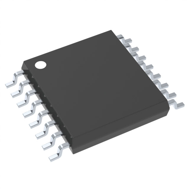
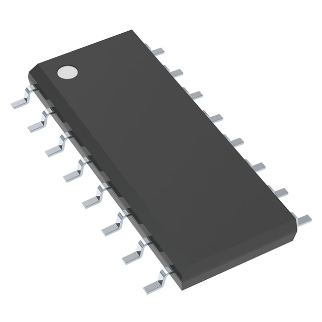
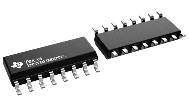
| Package Name | 16-SOIC |
| Package Width | 3.9 mm |
| PLL | Yes with Bypass |
| Type | PLL Clock Driver |
| Voltage - Supply (Maximum) | 3.6 V |
| Voltage - Supply (Minimum) | 3 V |
Pricing
Prices provided here are for design reference only. For realtime values and availability, please visit the distributors directly
Sign in to see pricing
Create a free account to access distributor pricing data.
CAD
3D models and CAD resources for this part
Documents
Technical documentation and resources