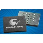
Description
General part information
S26KS512 Series
S26KS512SDPBHV020 is a S26KS512S HYPERFLASH™ high-speed CMOS, MIRRORBIT™ NOR flash device with the HYPERBUS™ low signal count DDR interface, that achieves high speed read throughput. The DDR protocol transfers two data bytes per clock cycle on the data (DQ) signals. A read or write access for the HYPERFLASH™ consists of a series of 16-bit wide, one clock cycle data transfers at the internal HYPERFLASH™ core and two corresponding 8-bit wide, one-half-clock-cycle data transfers on the DQ signals. Command/address/write-data values are center aligned with the clock edges and read-data values are edge aligned with the transitions of RWDS. During linear operation accesses start at a selected location and continue in a sequential manner until the read operation is terminated, when CS# returns HIGH. Write transactions transfer one or more 16-bit values.
Technical Specifications
Parameters and characteristics for this part
| Specification | S26KS512SDPBHV020 |
|---|---|
| Access Time | 96 ns |
| Clock Frequency | 166 MHz |
| Memory Depth | 64 M |
| Memory Format | FLASH |
| Memory Interface (Type) | HyperBus |
| Memory Size | 512 Mb |
| Memory Type | Non-Volatile |
| Memory Width | 8 bit |
| Mounting Type | Surface Mount |
| Operating Temperature (Max) | 105 °C |
| Operating Temperature (Min) | -40 °C |
| Package / Case | 24-VBGA |
| Package Length | 6 mm |
| Package Name | 24-FBGA |
| Package Width | 8 mm |
| Technology | FLASH - NOR |
| Voltage - Supply (Maximum) | 1.95 V |
| Voltage - Supply (Minimum) | 1.7 V |
Pricing
Prices provided here are for design reference only. For realtime values and availability, please visit the distributors directly
Sign in to see pricing
Create a free account to access distributor pricing data.
CAD
3D models and CAD resources for this part
Documents
Technical documentation and resources