


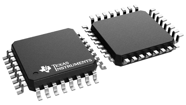
CDCLVD110AVFR
Active1-TO-10 LVDS CLOCK BUFFER UP TO 1100-MHZ WITH MINIMUM SKEW FOR CLOCK DISTRIBUTION

CDCLVD110AVFR
Active1-TO-10 LVDS CLOCK BUFFER UP TO 1100-MHZ WITH MINIMUM SKEW FOR CLOCK DISTRIBUTION
Description
General part information
CDCLVD110A Series
The CDCLVD110A clock driver distributes one pair of differential LVDS clock inputs (either CLK0 or CLK1) to 10 pairs of differential clock outputs (Q0 to Q9) with minimum skew for clock distribution. The CDCLVD110A is specifically designed to drive 50-Ω transmission lines.
When the control enable is high (EN = 1), the 10 differential outputs are programmable in that each output can be individually enabled or disabled(3-stated) according to the first 10 bits loaded into the shift register. Once the shift register is loaded, the last bit selects either CLK0 or CLK1 as the clock input. However, when EN = 0, the outputs are not programmable and all outputs are enabled.
The CDCLVD110A has an improved start-up circuit that minimizes enabling time in AC- and DC-coupled systems.
Technical Specifications
Parameters and characteristics for this part
| Specification | CDCLVD110AVFR |
|---|---|
| Differential Input | Yes |
| Differential Output | Yes |
| Frequency - Max | 1.1 GHz |
| Input | LVDS |
| Input Ratio | 2 |
| Mounting Type | Surface Mount |
| Number of Circuits | 1 |
| Operating Temperature (Max) | 85 °C |
| Operating Temperature (Min) | -40 °C |
| Output | LVDS |
| Output Ratio | 10 |
| Package / Case | 32-LQFP |
| Package Length | 7 mm |
| Package Name | 32-LQFP |
| Package Width | 7 mm |
| Type | Multiplexer, Fanout Buffer (Distribution) |
| Voltage - Supply (Maximum) | 2.625 V |
| Voltage - Supply (Minimum) | 2.375 V |
Pricing
Prices provided here are for design reference only. For realtime values and availability, please visit the distributors directly
Sign in to see pricing
Create a free account to access distributor pricing data.
CAD
3D models and CAD resources for this part
Documents
Technical documentation and resources