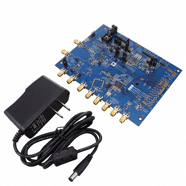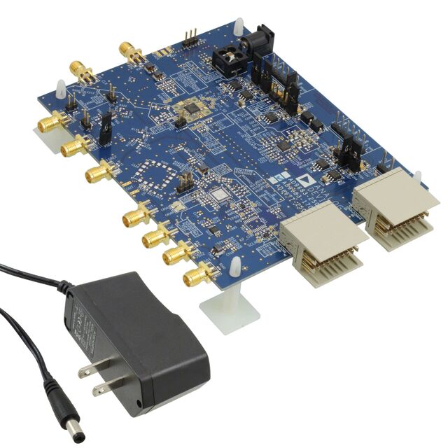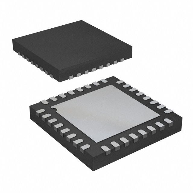
AD9683BCPZRL7-170
Active14-BIT, 170 MSPS/250 MSPS, JESD204B, ANALOG-TO-DIGITAL CONVERTER
AD9683BCPZRL7-170
Active14-BIT, 170 MSPS/250 MSPS, JESD204B, ANALOG-TO-DIGITAL CONVERTER
Description
General part information
AD9683 Series
The AD9683 is a 14-bit ADC with sampling speeds of up to 250 MSPS. The AD9683 supports communications applications where low cost, small size, wide bandwidth, and versatility are desired. The ADC core features a multistage, differential pipelined architecture with integrated output error correction logic. The ADC core features wide bandwidth inputs supporting a variety of user-selectable input ranges. An integrated voltage reference eases design considerations. A duty cycle stabilizer (DCS) is provided to compensate for variations in the ADC clock duty cycle, allowing the converter to maintain excellent performance. The JESD204B high speed serial interface reduces board routing requirements and lowers pin count requirements for the receiving device. The ADC output data is routed directly to the JESD204B serial output lane. These outputs are at CML voltage levels. Data can be sent through the lane at the maximum sampling rate of 250 MSPS, which results in a lane rate of 5 Gbps. Synchronization inputs (SYNCINB± and SYSREF±) are provided. Flexible power-down options allow significant power savings, when desired. Programmable overrange level detection is supported via the dedicated fast detect pins. Programming for setup and control is accomplished using a 3-wire SPI-compatible serial interface. The AD9683 is available in a 32-lead LFCSP and is specified over the industrial temperature range of −40°C to +85°C.Product HighlightsIntegrated 14-bit, 170 MSPS/250 MSPS ADC.The configurable JESD204B output block supports lane rates up to 5 Gbps.An on-chip, phase-locked loop (PLL) allows users to provide a single ADC sampling clock; the PLL multiplies the ADC sampling clock to produce the corresponding JESD204B data rate clock.Support for an optional radio frequency (RF) clock input to ease system board design.Proprietary differential input maintains excellent SNR performance for input frequencies of up to 400 MHz.Operation from a single 1.8 V power supply.Standard serial port interface (SPI) that supports various product features and functions, such as controlling the clock DCS, power-down, test modes, voltage reference mode, overrange fast detection, and serial output configuration.ApplicationsCommunicationsDiversity radio systemsMultimode digital receivers (3G)TD-SCDMA, WiMAX, W-CDMA, CDMA2000, GSM, EDGE, LTEDOCSIS 3.0 CMTS upstream receive pathsHFC digital reverse path receiversSmart antenna systemsElectronic test and measurement equipmentRadar receiversCOMSEC radio architecturesIED detection/jamming systemsGeneral-purpose software radiosBroadband data applicationsUltrasound equipment
Technical Specifications
Parameters and characteristics for this part
| Specification | AD9683BCPZRL7-170 |
|---|---|
| Architecture | Pipelined |
| Configuration | ADC |
| Data Interface | JESD204B |
| Input Type | Differential |
| Mounting Type | Surface Mount |
| Number of A/D Converters | 1 count |
| Number of Bits | 14 bits |
| Number of Inputs | 1 |
| Operating Temperature (Max) | 85 °C |
| Operating Temperature (Min) | -40 °C |
| Package / Case | 32-WFQFN Exposed Pad, CSP |
| Package Length | 5 mm |
| Package Name | 32-LFCSP |
| Package Width | 5 mm |
| Reference Type | Internal |
| Sampling Rate (Per Second) | 170 MHz |
| Voltage - Supply, Analog (Max) | 1.9 V |
| Voltage - Supply, Analog (Min) | 1.7 V |
| Voltage - Supply, Digital (Max) | 1.9 V |
| Voltage - Supply, Digital (Min) | 1.7 V |
Pricing
Prices provided here are for design reference only. For realtime values and availability, please visit the distributors directly
Sign in to see pricing
Create a free account to access distributor pricing data.
CAD
3D models and CAD resources for this part
Documents
Technical documentation and resources