


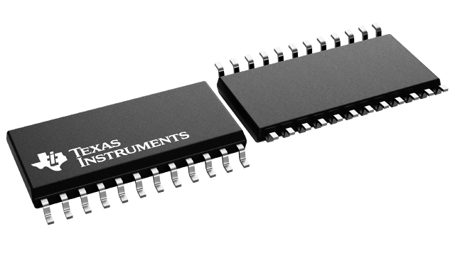
SN74LS673DW
ActiveSERIAL-IN SHIFT REGISTERS WITH OUTPUT STORAGE REGISTERS
SN74LS673DW
ActiveSERIAL-IN SHIFT REGISTERS WITH OUTPUT STORAGE REGISTERS
Description
General part information
74LS673 Series
SN54LS673, SN74LS673
The 'LS673 is a 16-bit shift register and a 16-bit storage register in a single 24-pin package. A three-state input/output (SER/Q15) port to the shift register allows serial entry and/or reading of data. The storage register is connected in a parallel data loop with the shift register and may be asynchronously cleared by taking the store-clear input low. The storage register may be parallel loaded with shift-register data to provide shift-register status via the parallel outputs. The shift register can be parallel loaded with the storage-register data upon commmand.
A high logic level at the chip-level (CS\) input disables both the shift-register clock and the storage register clock and places SER/Q15 in the high-impedance state. The store-clear function is not disabled by the chip select.
Technical Specifications
Parameters and characteristics for this part
| Specification | SN74LS673DW |
|---|---|
| Function | Serial to Parallel |
| Logic Type | Shift Register |
| Mounting Type | Surface Mount |
| Number of Bits per Element | 16 bits |
| Number of Elements | 1 |
| Operating Temperature (Max) | 70 °C |
| Operating Temperature (Min) | 0 °C |
| Output Type | Tri-State |
| Package Length | 0.295 in |
| Package Name | 24-SOIC |
| Package Width | 7.5 mm |
| Voltage - Supply (Maximum) | 5.25 V |
| Voltage - Supply (Minimum) | 4.75 V |
Pricing
Prices provided here are for design reference only. For realtime values and availability, please visit the distributors directly
Sign in to see pricing
Create a free account to access distributor pricing data.
CAD
3D models and CAD resources for this part
Documents
Technical documentation and resources

