SN54LS75J
Active4-BIT BISTABLE LATCHES 16-CDIP -
SN54LS75J
Active4-BIT BISTABLE LATCHES 16-CDIP -
Description
General part information
SN54LS75 Series
These latches are ideally suited for use as temporary storage for binary information between processing units and input/output or indicator units. Information present at a data (D) input is transferred to the Q output when the enable (C) is high and the Q output will follow the data input as long as the enable remains high. When the enable goes low, the information (that was present at the data input at the time the transition occurred) is retained at the Q output until the enable is permitted to go high.
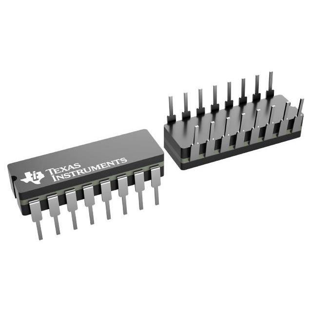
The '75 and 'LS75 feature complementary Q and Q\ outputs from a 4-bit latch, and are available in various 16-pin packages. For higher component density applications, the '77 and 'LS77 4-bit latches are available in 14-pin flat packages.
These circuits are completely compatible with all popular TTL families. All inputs are diode-clamped to minimize transmission-line effects and simplify system design. Series 54 and 54LS devices are characterized for operation over the full military temperature range of -55°C to 125°C; Series 74, and 74LS devices are characterized for operation from 0°C to 70°C.
Technical Specifications
Parameters and characteristics for this part
| Specification | SN54LS75J |
|---|---|
| Circuit | 2:2 |
| Current - Output High | 400 µA |
| Current - Output Low | 16 mA |
| Delay Time - Propagation | 15 ns |
| Independent Circuits | 2 |
| Logic Type | D-Type Transparent Latch |
| Mounting Type | Through Hole |
| Operating Temperature (Max) | 125 °C |
| Operating Temperature (Min) | -55 °C |
| Output Type | Complementary |
| Package Length | 0.3 in |
| Package Name | 16-CDIP |
| Package Width | 7.62 mm |
| Voltage - Supply (Maximum) | 5.5 V |
| Voltage - Supply (Minimum) | 4.5 V |
Pricing
Prices provided here are for design reference only. For realtime values and availability, please visit the distributors directly
Sign in to see pricing
Create a free account to access distributor pricing data.
CAD
3D models and CAD resources for this part
Documents
Technical documentation and resources