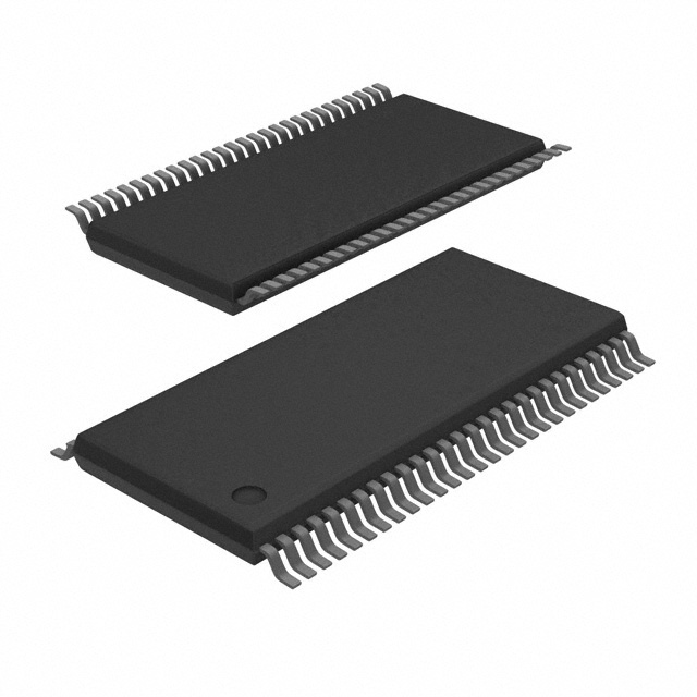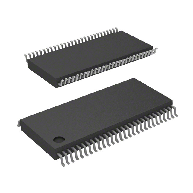
DS90CF384MTDX/NOPB
Active+3.3V LVDS RECEIVER 24-BIT FLAT PANEL DISPLAY (FPD) LINK-65 MHZ
DS90CF384MTDX/NOPB
Active+3.3V LVDS RECEIVER 24-BIT FLAT PANEL DISPLAY (FPD) LINK-65 MHZ
Description
General part information
DS90CF384 Series
The DS90C383 transmitter converts 28 bits of CMOS/TTL data into four LVDS (Low Voltage Differential Signaling) data streams. A phase-locked transmit clock is transmitted in parallel with the data streams over a fifth LVDS link. Every cycle of the transmit clock 28 bits of input data are sampled and transmitted. The DS90CF384 receiver converts the LVDS data streams back into 28 bits of CMOS/TTL data. At a transmit clock frequency of 65 MHz, 24 bits of RGB data and 3 bits of LCD timing and control data (FPLINE, FPFRAME, DRDY) are transmitted at a rate of 455 Mbps per LVDS data channel. Using a 65 MHz clock, the data throughputs is 227 Mbytes/sec. The transmitter is offered with programmable edge data strobes for convenient interface with a variety of graphics controllers. The transmitter can be programmed for Rising edge strobe or Falling edge strobe through a dedicated pin. A Rising edge transmitter will inter-operate with a Falling edge receiver (DS90CF384) without any translation logic. The DS90CF384 is also offered in 64 ball, 0.8mm fine pitch ball grid array(FBGA) package which provides a 44 % reduction in PCB footprint (available Q3, 1999).
This chipset is an ideal means to solve EMI and cable size problems associated with wide, high speed TTL interfaces.
The DS90C383 transmitter converts 28 bits of CMOS/TTL data into four LVDS (Low Voltage Differential Signaling) data streams. A phase-locked transmit clock is transmitted in parallel with the data streams over a fifth LVDS link. Every cycle of the transmit clock 28 bits of input data are sampled and transmitted. The DS90CF384 receiver converts the LVDS data streams back into 28 bits of CMOS/TTL data. At a transmit clock frequency of 65 MHz, 24 bits of RGB data and 3 bits of LCD timing and control data (FPLINE, FPFRAME, DRDY) are transmitted at a rate of 455 Mbps per LVDS data channel. Using a 65 MHz clock, the data throughputs is 227 Mbytes/sec. The transmitter is offered with programmable edge data strobes for convenient interface with a variety of graphics controllers. The transmitter can be programmed for Rising edge strobe or Falling edge strobe through a dedicated pin. A Rising edge transmitter will inter-operate with a Falling edge receiver (DS90CF384) without any translation logic. The DS90CF384 is also offered in 64 ball, 0.8mm fine pitch ball grid array(FBGA) package which provides a 44 % reduction in PCB footprint (available Q3, 1999).
Technical Specifications
Parameters and characteristics for this part
| Specification | DS90CF384MTDX/NOPB |
|---|---|
| Mounting Type | Surface Mount |
| Package Length | 0.24 in |
| Package Name | 56-TSSOP, 56-TFSOP |
| Package Width | 6.1 mm |
| Voltage - Supply (Maximum) | 3.6 V |
| Voltage - Supply (Minimum) | 3 V |
Pricing
Prices provided here are for design reference only. For realtime values and availability, please visit the distributors directly
Sign in to see pricing
Create a free account to access distributor pricing data.
CAD
3D models and CAD resources for this part
Documents
Technical documentation and resources