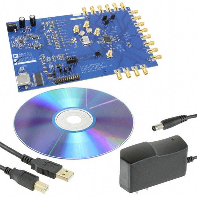
AD9523-1BCPZ
ActiveLOW JITTER CLOCK GENERATOR WITH 14 LVPECL/LVDS/HSTL/29 LVCMOS OUTPUTS
AD9523-1BCPZ
ActiveLOW JITTER CLOCK GENERATOR WITH 14 LVPECL/LVDS/HSTL/29 LVCMOS OUTPUTS
Description
General part information
AD9523 Series
The AD9523-1 provides a low power, multi-output, clock distribution function with low jitter performance, along with an on-chip PLL and VCO with two VCO dividers. The on-chip VCO tunes from 2.94 GHz to 3.1 GHz.The AD9523-1 is designed to support the clock requirements for long term evolution (LTE) and multicarrier GSM base station designs. It relies on an external VCXO to provide the reference jitter cleanup to achieve the restrictive low phase noise requirements necessary for acceptable data converter SNR performance.The input receivers, oscillator, and zero delay receiver provide both single-ended and differential operation. When connected to a recovered system reference clock and a VCXO, the device generates 14 low noise outputs with a range of 1 MHz to 1 GHz, and one dedicated buffered output from the input PLL (PLL1). The frequency and phase of one clock output relative to another clock output can be varied by means of a divider phase select function that serves as a jitter-free, coarse timing adjustment in increments that are equal to half the period of the signal coming out of the VCO.An in-package EEPROM can be programmed through the serial interface to store user-defined register settings for power-up and chip reset.APPLICATIONSLTE and multicarrier GSM base stationsWireless and broadband infrastructureMedical instrumentationClocking high speed ADCs, DACs, DDSs, DDCs, DUCs, MxFEsLow jitter, low phase noise clock distributionClock generation and translation for SONET, 10Ge, 10G FC, and other 10 Gbps protocolsForward error correction (G.710)High performance wireless transceiversATE and high performance instrumentation
Technical Specifications
Parameters and characteristics for this part
| Specification | AD9523-1BCPZ |
|---|---|
| Differential Input | Yes |
| Differential Output | Yes |
| Frequency - Max | 1 GHz |
| Input | CMOS |
| Input Ratio | 2 |
| Main Purpose | Fibre Channel, Ethernet, SONET/SDH |
| Mounting Type | Surface Mount |
| Number of Circuits | 1 |
| Operating Temperature (Max) | 85 °C |
| Operating Temperature (Min) | -40 °C |
| Output | LVPECL, HSTL, LVCMOS, LVDS |
| Output Ratio | 14 |
| Package / Case | 72-VFQFN Exposed Pad, CSP |
| Package Length | 10 mm |
| Package Name | 72-LFCSP-VQ |
| Package Width | 10 mm |
| PLL | Yes |
| Voltage - Supply (Maximum) | 3.465 V |
| Voltage - Supply (Minimum) | 1.768 V |
Pricing
Prices provided here are for design reference only. For realtime values and availability, please visit the distributors directly
Sign in to see pricing
Create a free account to access distributor pricing data.
CAD
3D models and CAD resources for this part
Documents
Technical documentation and resources