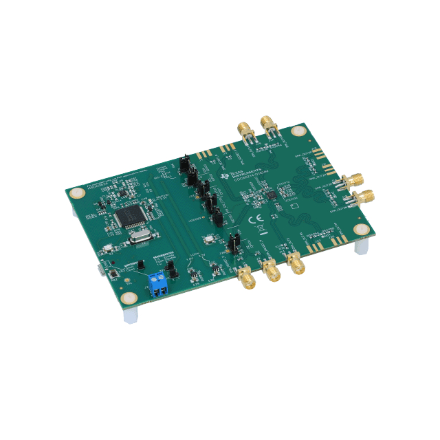
CDCE6214-Q1EVM
ActiveEVAL BOARD FOR DCE6214-Q1
Deep-Dive with AI
Search across all available documentation for this part.
CDCE6214-Q1EVM
ActiveEVAL BOARD FOR DCE6214-Q1
Deep-Dive with AI
Technical Specifications
Parameters and characteristics commom to parts in this series
| Specification | CDCE6214-Q1EVM | CDCE6214 Series |
|---|---|---|
| Differential - Input:Output | - | True |
| Differential - Input:Output | - | True |
| Divider/Multiplier | - | Yes/No |
| Frequency - Max | - | 328.125 - 350 MHz |
| Function | Clock Generator | Clock Generator |
| Grade | - | Automotive |
| Input | - | Differential or Single-Ended, Differential or Single-Ended, LVCMOS |
| Mounting Type | - | Surface Mount, Wettable Flank, Surface Mount |
| Number of Circuits | - | 1 |
| Operating Temperature | - | 85 - 105 °C |
| Operating Temperature | - | -40 °C |
| Output | - | HCSL, LVCMOS, LVDS, LP-HCSL |
| Package / Case | - | 24-VFQFN Exposed Pad |
| PLL | - | True |
| Qualification | - | AEC-Q100 |
| Ratio - Input:Output | - | 2 |
| Ratio - Input:Output | - | 4 - 5 |
| Secondary Attributes | USB Interface(s) | USB Interface(s) |
| Supplied Contents | Board(s) | Board(s) |
| Supplier Device Package | - | 24-VQFN (4x4) |
| Type | Timing | Clock Generator, Timing |
| Utilized IC / Part | DCE6214-Q1 | DCE6214-Q1 |
| Voltage - Supply | - | 3.465 V |
| Voltage - Supply | - | 1.71 V |
Pricing
Prices provided here are for design reference only. For realtime values and availability, please visit the distributors directly
| Distributor | Package | Quantity | $ | |
|---|---|---|---|---|
| Digikey | Box | 1 | $ 238.80 | |
CDCE6214 Series
Ultra-low power clock generator with one PLL, four differential output
| Part | Qualification | Mounting Type | Divider/Multiplier | Grade | Output | Number of Circuits | Package / Case | Operating Temperature [Max] | Operating Temperature [Min] | Voltage - Supply [Max] | Voltage - Supply [Min] | PLL | Frequency - Max [Max] | Type | Input | Supplier Device Package | Function | Utilized IC / Part | Secondary Attributes | Supplied Contents | Differential - Input:Output [custom] | Differential - Input:Output [custom] | Ratio - Input:Output [custom] | Ratio - Input:Output [custom] |
|---|---|---|---|---|---|---|---|---|---|---|---|---|---|---|---|---|---|---|---|---|---|---|---|---|
Texas Instruments CDCE6214TWRGETQ1 | AEC-Q100 | Surface Mount, Wettable Flank | Yes/No | Automotive | HCSL, LVCMOS, LVDS | 1 | 24-VFQFN Exposed Pad | 105 °C | -40 °C | 3.465 V | 1.71 V | 350 MHz | Clock Generator | Differential or Single-Ended | 24-VQFN (4x4) | |||||||||
Texas Instruments CDCE6214TWRGERQ1 | AEC-Q100 | Surface Mount, Wettable Flank | Yes/No | Automotive | HCSL, LVCMOS, LVDS | 1 | 24-VFQFN Exposed Pad | 105 °C | -40 °C | 3.465 V | 1.71 V | 350 MHz | Clock Generator | Differential or Single-Ended | 24-VQFN (4x4) | |||||||||
Texas Instruments CDCE6214-Q1EVM | Timing | Clock Generator | DCE6214-Q1 | USB Interface(s) | Board(s) | |||||||||||||||||||
Texas Instruments CDCE6214RGER | Surface Mount | Yes/No | LP-HCSL, LVCMOS, LVDS | 1 | 24-VFQFN Exposed Pad | 105 °C | -40 °C | 3.465 V | 1.71 V | 328.125 MHz | Clock Generator | Differential or Single-Ended, LVCMOS | 24-VQFN (4x4) | 2 | 5 | |||||||||
Texas Instruments CDCE6214RGET | Surface Mount, Wettable Flank | Yes/No | LP-HCSL, LVCMOS, LVDS | 1 | 24-VFQFN Exposed Pad | 85 °C | -40 °C | 3.465 V | 1.71 V | 350 MHz | Clock Generator | Differential or Single-Ended | 24-VQFN (4x4) | 2 | 4 |
Description
General part information
CDCE6214 Series
The CDCE6214 is a four-channel, ultra-low power, medium grade jitter, clock generator that can generate five independent clock outputs selectable between various modes of drivers. The input source could be a single-ended or differential input clock source, or a crystal. The CDCE6214 features a frac-N PLL to synthesize unrelated base frequency from any input frequency. The CDCE6214 can be configured through the I2C interface. In the absence of the serial interface, the GPIO pins can be used in Pin Mode to configure the product into distinctive configurations.
On-chip EEPROM can be used to change the configuration, which is pre-selectable through the pins. The device provides frequency margining options with glitch-free operation to support system design verification tests (DVT) and Ethernet Audio-Video Bridging (eAVB). Fine frequency margining is available on any output channel by steering the fractional feedback divider in DCO mode.
Internal power conditioning provides excellent power supply ripple rejection (PSRR), reducing the cost and complexity of the power delivery network. The analog and digital core blocks operate from either a 1.8-V, 2.5-V, or 3.3-V ±5% supply, and output blocks operate from a 1.8-V, 2.5-V, or 3.3-V ±5% supply.
Documents
Technical documentation and resources