


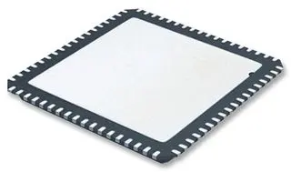
AD9094BCPZ-1000
ActiveANALOG TO DIGITAL CONVERTER, 8 BIT, 1 GSPS, DIFFERENTIAL, PARALLEL, SINGLE, 877 MV
AD9094BCPZ-1000
ActiveANALOG TO DIGITAL CONVERTER, 8 BIT, 1 GSPS, DIFFERENTIAL, PARALLEL, SINGLE, 877 MV
Description
General part information
AD9094 Series
The AD9094 is an 8-bit, 1 GSPS, quad analog-to-digital converter (ADC). The device has an on-chip buffer and a sample-and-hold circuit designed for low power, small size, and ease of use. The device is designed to sample wide bandwidth analog signals up to 1.4 GHz. The AD9094 is optimized for wide input bandwidth, a high sampling rate, high works linearity, and low power in a small package.The quad-ADC cores feature multistage, differential pipelined architecture with integrated output error correction logic. Each ADC features wide bandwidth inputs that support a variety of user-selectable input ranges. An integrated voltage reference facilitates design considerations. The analog inputs and clock signals are differential inputs.Users can configure each pair of intermediate frequency (IF) receiver outputs onto either one or two lanes of JESD204B Subclass 1 or Subclass 0, high speed, serialized outputs, depending on the sample rate and the acceptable lane rate of the receiving logic device. Multiple device synchronization is supported through the SYSREF±, SYNCINB±AB, and SYNCINB±CD input pins.The AD9094 has flexible power-down options that allow significant power savings when desired. To program the power down options, use the 1.8 V capable, serial port interface (SPI).The AD9094 is available in a Pb-free, 72-lead, lead frame chip scale package (LFCSP) and is specified over a junction temperature range of −40°C to +105°C. This product may be protected by one or more U.S. or international patents.Note that throughout the data sheet, multifunction pins, such as PDWN/STBY, are referred to either by the entire pin name or by a single function of the pin, for example, PDWN, when only that function is relevant.Product HighlightsLow power consumption per channel.JESD204B lane rate support up to 15 Gbps.Wide, full power bandwidth supports IF sampling of signals up to 1.4 GHz.Buffered inputs ease filter design and implementation.Four integrated wideband decimation filters and numerically controlled oscillator (NCO) blocks supporting multiband receivers.Programmable fast overrange detection.On-chip temperature diode for system thermal management.ApplicationsLaser imaging, detection, and ranging (LIDAR)CommunicationsDigital oscilloscope (DSO)Ultrawideband satellite receiversInstrumentation
Technical Specifications
Parameters and characteristics for this part
| Specification | AD9094BCPZ-1000 |
|---|---|
| Architecture | Pipelined |
| Configuration | S/H-ADC |
| Data Interface | SPI, Parallel, JESD204B |
| Input Type | Differential |
| Mounting Type | Surface Mount |
| Number of A/D Converters | 4 count |
| Number of Bits | 8 bits |
| Number of Inputs | 4 |
| Operating Temperature (Max) | 105 °C |
| Operating Temperature (Min) | -40 °C |
| Package / Case | 72-VFQFN Exposed Pad, CSP |
| Package Length | 10 mm |
| Package Name | 72-LFCSP-VQ |
| Package Width | 10 mm |
| Ratio - ADC | 1 |
| Ratio - S/H | 1 |
| Reference Type | External, Internal |
| Sampling Rate (Per Second) | 1 GHz |
| Voltage - Supply, Analog (Range 1 Max) | 1 V |
| Voltage - Supply, Analog (Range 1 Min) | 0.95 V |
| Voltage - Supply, Analog (Range 2 Max) | 1.89 V |
| Voltage - Supply, Analog (Range 2 Min) | 1.71 V |
| Voltage - Supply, Analog (Range 3 Max) | 2.56 V |
| Voltage - Supply, Analog (Range 3 Min) | 2.44 V |
| Voltage - Supply, Digital (Range 1) Maximum | 1 V |
| Voltage - Supply, Digital (Range 1) Minimum | 0.95 V |
| Voltage - Supply, Digital (Range 2) Maximum | 1.89 V |
| Voltage - Supply, Digital (Range 2) Minimum | 1.71 V |
Pricing
Prices provided here are for design reference only. For realtime values and availability, please visit the distributors directly
Sign in to see pricing
Create a free account to access distributor pricing data.
CAD
3D models and CAD resources for this part
Documents
Technical documentation and resources


