CDCLVD2106RHAR
ActiveLOW JITTER, DUAL 1:6 UNIVERSAL-TO-LVDS BUFFER
Deep-Dive with AI
Search across all available documentation for this part.
CDCLVD2106RHAR
ActiveLOW JITTER, DUAL 1:6 UNIVERSAL-TO-LVDS BUFFER
Deep-Dive with AI
Technical Specifications
Parameters and characteristics commom to parts in this series
| Specification | CDCLVD2106RHAR | CDCLVD2106 Series |
|---|---|---|
| Differential - Input:Output [custom] | True | True |
| Differential - Input:Output [custom] | True | True |
| Embedded | - | False |
| Frequency - Max [Max] | 800 MHz | 800 MHz |
| Function | - | Clock Buffer |
| Input | LVPECL, LVCMOS, LVDS | LVPECL, LVCMOS, LVDS |
| Mounting Type | Surface Mount | Surface Mount |
| Number of Circuits | 2 | 2 |
| Operating Temperature [Max] | 85 °C | 85 °C |
| Operating Temperature [Min] | -40 °C | -40 °C |
| Output | LVDS | LVDS |
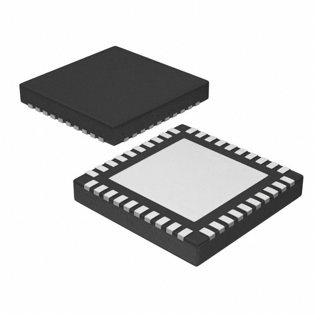
| Package / Case | 40-VFQFN Exposed Pad | 40-VFQFN Exposed Pad |
| Primary Attributes | - | 4 - 12 Ports |
| Ratio - Input:Output [custom] | 6 | 6 |
| Ratio - Input:Output [custom] | 1 | 1 |
| Supplied Contents | - | Board(s) |
| Supplier Device Package | 40-VQFN (6x6) | 40-VQFN (6x6) |
| Type | Fanout Buffer (Distribution) | Fanout Buffer (Distribution), Timing |
| Utilized IC / Part | - | CDCLVD2106 |
| Voltage - Supply [Max] | 2.625 V | 2.625 V |
| Voltage - Supply [Min] | 2.375 V | 2.375 V |
Pricing
Prices provided here are for design reference only. For realtime values and availability, please visit the distributors directly
| Distributor | Package | Quantity | $ | |
|---|---|---|---|---|
| Digikey | Tape & Reel (TR) | 2500 | $ 6.07 | |
| Texas Instruments | LARGE T&R | 1 | $ 8.50 | |
| 100 | $ 6.93 | |||
| 250 | $ 5.45 | |||
| 1000 | $ 4.62 | |||
CDCLVD2106 Series
Low jitter, dual 1:6 universal-to-LVDS buffer
| Part | Package / Case | Ratio - Input:Output [custom] | Ratio - Input:Output [custom] | Differential - Input:Output [custom] | Differential - Input:Output [custom] | Voltage - Supply [Min] | Voltage - Supply [Max] | Supplier Device Package | Frequency - Max [Max] | Input | Number of Circuits | Mounting Type | Output | Type | Operating Temperature [Min] | Operating Temperature [Max] | Utilized IC / Part | Supplied Contents | Embedded | Function | Primary Attributes |
|---|---|---|---|---|---|---|---|---|---|---|---|---|---|---|---|---|---|---|---|---|---|
Texas Instruments CDCLVD2106RHAT | 40-VFQFN Exposed Pad | 6 | 1 | 2.375 V | 2.625 V | 40-VQFN (6x6) | 800 MHz | LVCMOS, LVDS, LVPECL | 2 | Surface Mount | LVDS | Fanout Buffer (Distribution) | -40 °C | 85 °C | |||||||
Texas Instruments CDCLVD2106RHAR | 40-VFQFN Exposed Pad | 6 | 1 | 2.375 V | 2.625 V | 40-VQFN (6x6) | 800 MHz | LVCMOS, LVDS, LVPECL | 2 | Surface Mount | LVDS | Fanout Buffer (Distribution) | -40 °C | 85 °C | |||||||
Texas Instruments CDCLVD2106EVM | Timing | CDCLVD2106 | Board(s) | Clock Buffer | 4 Ports, 12 Outputs |
Description
General part information
CDCLVD2106 Series
The CDCLVD2106 clock buffer distributes two clock inputs (IN0, IN1) to a total of 12 pairs of differential LVDS clock outputs (OUT0, OUT11). Each buffer block consists of one input and 6 LVDS outputs. The inputs can either be LVDS, LVPECL, or LVCMOS.
The CDCLVD2106 is specifically designed for driving 50-Ω transmission lines. In case of driving the inputs in single ended mode, the appropriate bias voltage (VAC_REF) should be applied to the unused negative input pin.
Using the control pin (EN), outputs can be either disabled or enabled. If the EN pin is left open two buffers with all outputs are enabled, if switched to a logical "0" both buffers with all outputs are disabled (static logical "0"), if switched to a logical "1", one buffer with six outputs is disabled and another buffer with six outputs is enabled. The part supports a fail safe function. It incorporates an input hysteresis, which prevents random oscillation of the outputs in absence of an input signal.
Documents
Technical documentation and resources