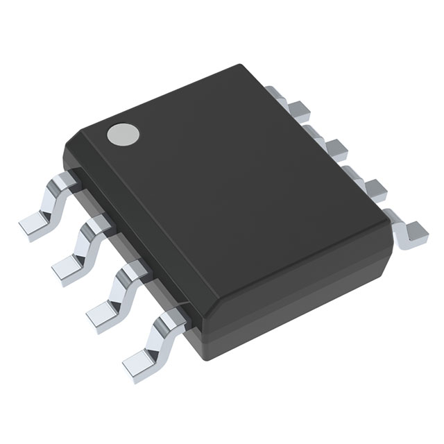
SN65LVDT34DR
ActiveQUAD LVDS RECEIVER WITH -4 TO 5-V COMMON-MODE RANGE
Deep-Dive with AI
Search across all available documentation for this part.

SN65LVDT34DR
ActiveQUAD LVDS RECEIVER WITH -4 TO 5-V COMMON-MODE RANGE
Deep-Dive with AI
Technical Specifications
Parameters and characteristics commom to parts in this series
| Specification | SN65LVDT34DR | 65LVDT34 Series |
|---|---|---|
| Data Rate | 400 Mbps | 400 Mbps |
| Mounting Type | Surface Mount | Surface Mount |
| Number of Drivers/Receivers [custom] | 2 | 2 |
| Number of Drivers/Receivers [custom] | 0 | 0 |
| Operating Temperature [Max] | 85 °C | 85 °C |
| Operating Temperature [Min] | -40 °C | -40 °C |
| Package / Case | 3.9 mm | 3.9 mm |
| Package / Case | 8-SOIC | 8-SOIC |
| Protocol | LVDS | LVDS |
| Receiver Hysteresis | 50 mV | 50 mV |
| Supplier Device Package | 8-SOIC | 8-SOIC |
| Type | Receiver | Receiver |
| Voltage - Supply [Max] | 3.6 V | 3.6 V |
| Voltage - Supply [Min] | 3 V | 3 V |
Pricing
Prices provided here are for design reference only. For realtime values and availability, please visit the distributors directly
65LVDT34 Series
Quad LVDS receiver with -4 to 5-V common-mode range
| Part | Type | Receiver Hysteresis | Voltage - Supply [Max] | Voltage - Supply [Min] | Operating Temperature [Min] | Operating Temperature [Max] | Mounting Type | Data Rate | Number of Drivers/Receivers [custom] | Number of Drivers/Receivers [custom] | Supplier Device Package | Protocol | Package / Case | Package / Case |
|---|---|---|---|---|---|---|---|---|---|---|---|---|---|---|
Texas Instruments SN65LVDT34DRThis family of four LVDS data line receivers offers the widest common-mode input voltage range in the industry. These receivers provide an input voltage range specification compatible with a 5-V PECL signal as well as an overall increased ground-noise tolerance. They are in industry standard footprints with integrated termination as an option.
Precise control of the differential input voltage thresholds allows for inclusion of 50 mV of input voltage hysteresis to improve noise rejection on slowly changing input signals. The input thresholds are still no more than ±50 mV over the full input common-mode voltage range.
The high-speed switching of LVDS signals usually necessitates the use of a line impedance matching resistor at the receiving-end of the cable or transmission media. The SN65LVDT series of receivers eliminates this external resistor by integrating it with the receiver. The nonterminated SN65LVDS series is also available for multidrop or other termination circuits.
The receivers can withstand ±15 kV human-body model (HBM) and ±600 V machine model (MM) electrostatic discharges to the receiver input pins with respect to ground without damage. This provides reliability in cabled and other connections where potentially damaging noise is always a threat.
The receivers also include a (patent pending) failsafe circuit that will provide a high-level output within 600 ns after loss of the input signal. The most common causes of signal loss are disconnected cables, shorted lines, or powered-down transmitters. The failsafe circuit prevents noise from being received as valid data under these fault conditions. This feature may also be used for Wired-Or bus signaling. SeeThe Active Failsafe Feature of the SN65LVDS32Bapplication note.
The intended application and signaling technique of these devices is point-to-point baseband data transmission over controlled impedance media of approximately 100. The transmission media may be printed-circuit board traces, backplanes, or cables. The ultimate rate and distance of data transfer is dependent upon the attenuation characteristics of the media and the noise coupling to the environment.
The SN65LVDS33, SN65LVDT33, SN65LVDS34 and SN65LVDT34 are characterized for operation from –40°C to 85°C.
This family of four LVDS data line receivers offers the widest common-mode input voltage range in the industry. These receivers provide an input voltage range specification compatible with a 5-V PECL signal as well as an overall increased ground-noise tolerance. They are in industry standard footprints with integrated termination as an option.
Precise control of the differential input voltage thresholds allows for inclusion of 50 mV of input voltage hysteresis to improve noise rejection on slowly changing input signals. The input thresholds are still no more than ±50 mV over the full input common-mode voltage range.
The high-speed switching of LVDS signals usually necessitates the use of a line impedance matching resistor at the receiving-end of the cable or transmission media. The SN65LVDT series of receivers eliminates this external resistor by integrating it with the receiver. The nonterminated SN65LVDS series is also available for multidrop or other termination circuits.
The receivers can withstand ±15 kV human-body model (HBM) and ±600 V machine model (MM) electrostatic discharges to the receiver input pins with respect to ground without damage. This provides reliability in cabled and other connections where potentially damaging noise is always a threat.
The receivers also include a (patent pending) failsafe circuit that will provide a high-level output within 600 ns after loss of the input signal. The most common causes of signal loss are disconnected cables, shorted lines, or powered-down transmitters. The failsafe circuit prevents noise from being received as valid data under these fault conditions. This feature may also be used for Wired-Or bus signaling. SeeThe Active Failsafe Feature of the SN65LVDS32Bapplication note.
The intended application and signaling technique of these devices is point-to-point baseband data transmission over controlled impedance media of approximately 100. The transmission media may be printed-circuit board traces, backplanes, or cables. The ultimate rate and distance of data transfer is dependent upon the attenuation characteristics of the media and the noise coupling to the environment.
The SN65LVDS33, SN65LVDT33, SN65LVDS34 and SN65LVDT34 are characterized for operation from –40°C to 85°C. | Receiver | 50 mV | 3.6 V | 3 V | -40 °C | 85 °C | Surface Mount | 400 Mbps | 2 | 0 | 8-SOIC | LVDS | 3.9 mm | 8-SOIC |
Texas Instruments SN65LVDT34DThis family of four LVDS data line receivers offers the widest common-mode input voltage range in the industry. These receivers provide an input voltage range specification compatible with a 5-V PECL signal as well as an overall increased ground-noise tolerance. They are in industry standard footprints with integrated termination as an option.
Precise control of the differential input voltage thresholds allows for inclusion of 50 mV of input voltage hysteresis to improve noise rejection on slowly changing input signals. The input thresholds are still no more than ±50 mV over the full input common-mode voltage range.
The high-speed switching of LVDS signals usually necessitates the use of a line impedance matching resistor at the receiving-end of the cable or transmission media. The SN65LVDT series of receivers eliminates this external resistor by integrating it with the receiver. The nonterminated SN65LVDS series is also available for multidrop or other termination circuits.
The receivers can withstand ±15 kV human-body model (HBM) and ±600 V machine model (MM) electrostatic discharges to the receiver input pins with respect to ground without damage. This provides reliability in cabled and other connections where potentially damaging noise is always a threat.
The receivers also include a (patent pending) failsafe circuit that will provide a high-level output within 600 ns after loss of the input signal. The most common causes of signal loss are disconnected cables, shorted lines, or powered-down transmitters. The failsafe circuit prevents noise from being received as valid data under these fault conditions. This feature may also be used for Wired-Or bus signaling. SeeThe Active Failsafe Feature of the SN65LVDS32Bapplication note.
The intended application and signaling technique of these devices is point-to-point baseband data transmission over controlled impedance media of approximately 100. The transmission media may be printed-circuit board traces, backplanes, or cables. The ultimate rate and distance of data transfer is dependent upon the attenuation characteristics of the media and the noise coupling to the environment.
The SN65LVDS33, SN65LVDT33, SN65LVDS34 and SN65LVDT34 are characterized for operation from –40°C to 85°C.
This family of four LVDS data line receivers offers the widest common-mode input voltage range in the industry. These receivers provide an input voltage range specification compatible with a 5-V PECL signal as well as an overall increased ground-noise tolerance. They are in industry standard footprints with integrated termination as an option.
Precise control of the differential input voltage thresholds allows for inclusion of 50 mV of input voltage hysteresis to improve noise rejection on slowly changing input signals. The input thresholds are still no more than ±50 mV over the full input common-mode voltage range.
The high-speed switching of LVDS signals usually necessitates the use of a line impedance matching resistor at the receiving-end of the cable or transmission media. The SN65LVDT series of receivers eliminates this external resistor by integrating it with the receiver. The nonterminated SN65LVDS series is also available for multidrop or other termination circuits.
The receivers can withstand ±15 kV human-body model (HBM) and ±600 V machine model (MM) electrostatic discharges to the receiver input pins with respect to ground without damage. This provides reliability in cabled and other connections where potentially damaging noise is always a threat.
The receivers also include a (patent pending) failsafe circuit that will provide a high-level output within 600 ns after loss of the input signal. The most common causes of signal loss are disconnected cables, shorted lines, or powered-down transmitters. The failsafe circuit prevents noise from being received as valid data under these fault conditions. This feature may also be used for Wired-Or bus signaling. SeeThe Active Failsafe Feature of the SN65LVDS32Bapplication note.
The intended application and signaling technique of these devices is point-to-point baseband data transmission over controlled impedance media of approximately 100. The transmission media may be printed-circuit board traces, backplanes, or cables. The ultimate rate and distance of data transfer is dependent upon the attenuation characteristics of the media and the noise coupling to the environment.
The SN65LVDS33, SN65LVDT33, SN65LVDS34 and SN65LVDT34 are characterized for operation from –40°C to 85°C. | Receiver | 50 mV | 3.6 V | 3 V | -40 °C | 85 °C | Surface Mount | 400 Mbps | 2 | 0 | 8-SOIC | LVDS | 3.9 mm | 8-SOIC |
Receiver | 50 mV | 3.6 V | 3 V | -40 °C | 85 °C | Surface Mount | 400 Mbps | 2 | 0 | 8-SOIC | LVDS | 3.9 mm | 8-SOIC |
Description
General part information
65LVDT34 Series
This family of four LVDS data line receivers offers the widest common-mode input voltage range in the industry. These receivers provide an input voltage range specification compatible with a 5-V PECL signal as well as an overall increased ground-noise tolerance. They are in industry standard footprints with integrated termination as an option.
Precise control of the differential input voltage thresholds allows for inclusion of 50 mV of input voltage hysteresis to improve noise rejection on slowly changing input signals. The input thresholds are still no more than ±50 mV over the full input common-mode voltage range.
The high-speed switching of LVDS signals usually necessitates the use of a line impedance matching resistor at the receiving-end of the cable or transmission media. The SN65LVDT series of receivers eliminates this external resistor by integrating it with the receiver. The nonterminated SN65LVDS series is also available for multidrop or other termination circuits.
Documents
Technical documentation and resources


