UCC27524A1QDGNRQ1
ActiveAUTOMOTIVE 5-A/5-A DUAL-CHANNEL GATE DRIVER WITH 5-V UVLO AND NEGATIVE INPUT VOLTAGE HANDLING
UCC27524A1QDGNRQ1
ActiveAUTOMOTIVE 5-A/5-A DUAL-CHANNEL GATE DRIVER WITH 5-V UVLO AND NEGATIVE INPUT VOLTAGE HANDLING
Description
General part information
UCC27524 Series
The UCC27524A-Q1 device is a dual-channel, high-speed, low-side, gate-driver device capable of effectively driving MOSFET and IGBT power switches. The UCC27524A-Q1 device is a variant of the UCC2752x family. The UCC27524A-Q1 device adds the ability to handle –5V directly at the input pins for increased robustness. The UCC27524A-Q1 device is a dual, non-inverting driver. Using a design that inherently minimizes shoot-through current, the UCC27524A-Q1 device is capable of delivering high-peak current pulses of up to 5A source and 5A sink into capacitive loads along with rail-to-rail drive capability and extremely small propagation delay (typically 17ns). In addition, the drivers feature matched, internal-propagation delays between the two channels which are very well suited for applications requiring dual-gate drives with critical timing, such as synchronous rectifiers. This also enables connecting two channels in parallel to effectively increase current-drive capability or driving two switches in parallel with a single input signal. The input pin thresholds are based on TTL and CMOS compatible low-voltage logic, which is fixed and independent of the VDD supply voltage. Wide hysteresis between the high and low thresholds offers excellent noise immunity.
For protection purposes, internal pull-up and pull-down resistors on the input pins of the UCC27524A-Q1 device ensure that outputs are held LOW when input pins are in floating condition. The UCC27524A-Q1 device features enable pins (ENA and ENB) to have better control of the operation of the driver applications. The pins are internally pulled up to VDD for active-high logic and are left open for standard operation.
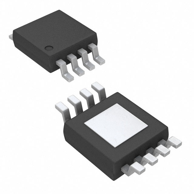
The UCC27524A-Q1 devices is available in SOIC-8 (D) and VSSOP-PowerPAD-8 with exposed pad (DGN) packages.
Technical Specifications
Parameters and characteristics for this part
| Specification | UCC27524A1QDGNRQ1 |
|---|---|
| Channel Type | Independent |
| Current - Peak Output (Sink) | 5 A |
| Current - Peak Output (Source) | 5 A |
| Driven Configuration | Low-Side |
| Fall Time (Typ) | 6 ns |
| Gate Channel | N-Channel |
| Gate Type | IGBT, MOSFET, N-Channel MOSFET |
| Grade | Automotive |
| Input Type | Non-Inverting |
| Logic Voltage - VIH | 2.3 V |
| Logic Voltage - VIL | 1 V |
| Mounting Type | Surface Mount |
| Number of Drivers | 2 |
| Operating Temperature (Max) | 140 °C |
| Operating Temperature (Min) | -40 °C |
| Package Features | Exposed Pad |
| Package Length | 0.118 in |
| Package Name | 8-HVSSOP, 8-MSOP, 8-TSSOP |
| Package Width | 3 mm |
| Qualification | AEC-Q100 |
| Rise Time (Typ) | 7 ns |
| Voltage - Supply (Maximum) | 18 V |
| Voltage - Supply (Minimum) | 4.5 V |
Pricing
Prices provided here are for design reference only. For realtime values and availability, please visit the distributors directly
Sign in to see pricing
Create a free account to access distributor pricing data.
CAD
3D models and CAD resources for this part
Documents
Technical documentation and resources