CDCLVP1102EVM
ActiveEVALUATION MODULE FOR CDCLVP1102
Deep-Dive with AI
Search across all available documentation for this part.
CDCLVP1102EVM
ActiveEVALUATION MODULE FOR CDCLVP1102
Deep-Dive with AI
Technical Specifications
Parameters and characteristics commom to parts in this series
| Specification | CDCLVP1102EVM | CDCLVP1102 Series |
|---|---|---|
| Differential - Input:Output | - | True |
| Differential - Input:Output | - | True |
| Embedded | False | False |
| Frequency - Max | - | 2 GHz |
| Function | Clock Buffer/Driver/Receiver/Translator | Clock Buffer/Driver/Receiver/Translator |
| Input | - | LVCMOS, LVTTL, LVPECL, LVDS |
| Mounting Type | - | Surface Mount |
| Number of Circuits | - | 1 |
| Operating Temperature | - | -40 °C |
| Operating Temperature | - | 85 °C |
| Output | - | LVPECL |
| Package / Case | - | 16-VFQFN Exposed Pad |
| Ratio - Input:Output | - | 1 |
| Ratio - Input:Output | - | 2 |
| Supplied Contents | Board(s) | Board(s) |
| Supplier Device Package | - | 16-VQFN (3x3) |
| Type | Timing | Fanout Buffer (Distribution), Timing |
| Utilized IC / Part | CDCLVP1102 | CDCLVP1102 |
| Voltage - Supply | - | 2.375 V |
| Voltage - Supply | - | 3.6 V |
Pricing
Prices provided here are for design reference only. For realtime values and availability, please visit the distributors directly
| Distributor | Package | Quantity | $ | |
|---|---|---|---|---|
| Digikey | Box | 1 | $ 178.80 | |
CDCLVP1102 Series
Low jitter 1:2 universal-to-LVPECL buffer
| Part | Ratio - Input:Output [custom] | Ratio - Input:Output [custom] | Supplier Device Package | Type | Input | Operating Temperature [Min] | Operating Temperature [Max] | Number of Circuits | Mounting Type | Differential - Input:Output [custom] | Differential - Input:Output [custom] | Frequency - Max [Max] | Output | Voltage - Supply [Min] | Voltage - Supply [Max] | Package / Case | Function | Supplied Contents | Embedded | Utilized IC / Part |
|---|---|---|---|---|---|---|---|---|---|---|---|---|---|---|---|---|---|---|---|---|
Texas Instruments CDCLVP1102RGTR | 1 | 2 | 16-VQFN (3x3) | Fanout Buffer (Distribution) | LVCMOS, LVDS, LVPECL, LVTTL | -40 °C | 85 °C | 1 | Surface Mount | 2 GHz | LVPECL | 2.375 V | 3.6 V | 16-VFQFN Exposed Pad | ||||||
Texas Instruments CDCLVP1102RGTT | 1 | 2 | 16-VQFN (3x3) | Fanout Buffer (Distribution) | LVCMOS, LVDS, LVPECL, LVTTL | -40 °C | 85 °C | 1 | Surface Mount | 2 GHz | LVPECL | 2.375 V | 3.6 V | 16-VFQFN Exposed Pad | ||||||
Texas Instruments CDCLVP1102EVM | Timing | Clock Buffer/Driver/Receiver/Translator | Board(s) | CDCLVP1102 |
Description
General part information
CDCLVP1102 Series
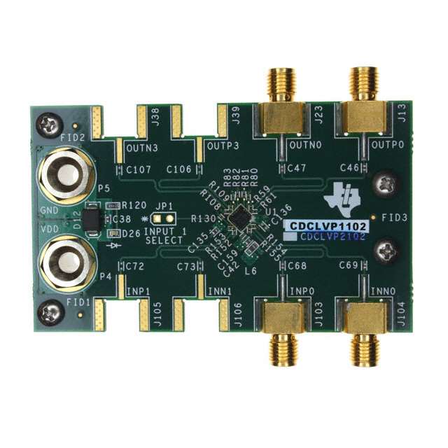
The CDCLVP1102 is a highly versatile, low additive jitter buffer that can generate two copies of LVPECL clock outputs from one LVPECL, LVDS, or LVCMOS input for a variety of communication applications. It has a maximum clock frequency up to 2 GHz. The overall additive jitter performance is less than 0.1 ps, RMS from 10 kHz to 20 MHz, and overall output skew is as low as 10 ps, making the device a perfect choice for use in demanding applications.
The CDCLVP1102 clock buffer distributes a single clock input (IN) to two pairs of differential LVPECL clock outputs (OUT0, OUT1) with minimum skew for clock distribution. The inputs can be LVPECL, LVDS, or LVCMOS/LVTTL.
The CDCLVP1102 is specifically designed for driving 50-Ω transmission lines. When driving the inputs in single-ended mode, the LVPECL bias voltage (VAC_REF) should be applied to the unused negative input pin. However, for high-speed performance up to 2 GHz, differential mode is strongly recommended.
Documents
Technical documentation and resources