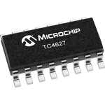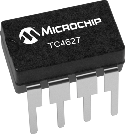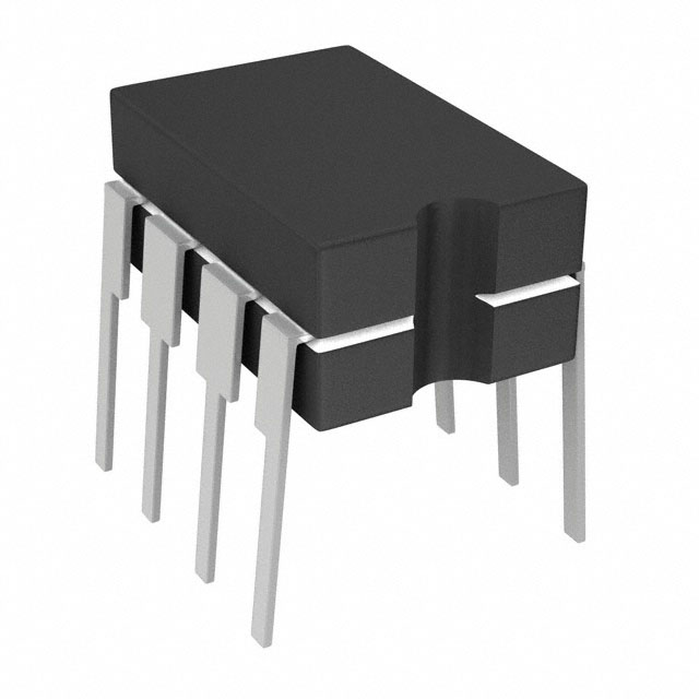
TC4627MJA
ActiveIC GATE DRVR HI/LOW SIDE 8CERDIP
TC4627MJA
ActiveIC GATE DRVR HI/LOW SIDE 8CERDIP
Description
General part information
TC4627 Series
The TC4626/4627 are single CMOS high speed gate drivers with an on-board voltage boost circuit. These parts work with an input supply voltage from 4 to 6 V. The internal voltage booster will produce a VBOOST potential up to 12 V above VIN. This VBOOST is not regulated, so its voltage is dependent on the input VDD voltage and output drive loading requirements. An internal under voltage lockout (UVLO) circuit keeps the output in a low state when VBOOST drops below 7.8 V. Output is enabled when VBOOST is above 11.3 V.
Technical Specifications
Parameters and characteristics for this part
| Specification | TC4627MJA |
|---|---|
| Channel Type | Single |
| Current - Peak Output (Sink) | 1.5 A |
| Current - Peak Output (Source) | 1.5 A |
| Driven Configuration | Low-Side, High-Side |
| Fall Time (Typ) | 27 ns |
| Gate Channel | N-Channel, P-Channel |
| Gate Type | N-Channel, P-Channel MOSFET, MOSFET |
| Input Type | Non-Inverting |
| Logic Voltage - VIH | 2.4 V |
| Logic Voltage - VIL | 0.8 V |
| Mounting Type | Through Hole |
| Number of Drivers | 1 |
| Operating Temperature (Max) | 125 °C |
| Operating Temperature (Min) | -55 °C |
| Package Length | 0.3 in |
| Package Name | 8-CDIP, 8-CERDIP |
| Package Width | 7.62 mm |
| Rise Time (Typ) | 33 ns |
| Voltage - Supply (Maximum) | 6 V |
| Voltage - Supply (Minimum) | 4 V |
Pricing
Prices provided here are for design reference only. For realtime values and availability, please visit the distributors directly
Sign in to see pricing
Create a free account to access distributor pricing data.
CAD
3D models and CAD resources for this part
Documents
Technical documentation and resources