Technical Specifications
Parameters and characteristics commom to parts in this series
| Specification | SN75LVDS82DGGRG4 | 75LVDS82 Series |
|---|---|---|
| Mounting Type | Surface Mount | Surface Mount |
| Number of Drivers/Receivers [custom] | 0 | 0 |
| Number of Drivers/Receivers [custom] | 5 | 5 |
| Operating Temperature [Max] | 70 ░C | 70 ░C |
| Operating Temperature [Min] | 0 °C | 0 °C |
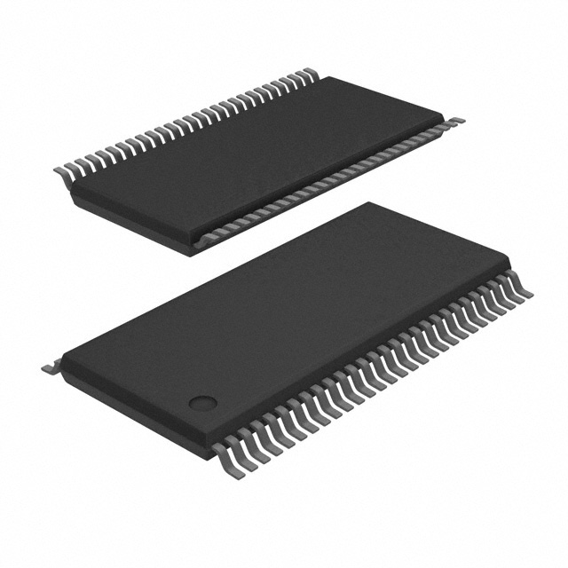
| Package / Case | 56-TFSOP | 56-TFSOP |
| Package / Case | 6.1 mm | 6.1 mm |
| Package / Case | 0.24 " | 0.24 " |
| Protocol | LVDS | LVDS |
| Supplier Device Package | 56-TSSOP | 56-TSSOP |
| Type | Receiver | Receiver |
| Voltage - Supply [Max] | 3.6 V | 3.6 V |
| Voltage - Supply [Min] | 3 V | 3 V |
Pricing
Prices provided here are for design reference only. For realtime values and availability, please visit the distributors directly
75LVDS82 Series
IC RECEIVER 0/5 56TSSOP
| Part | Type | Protocol | Supplier Device Package | Package / Case | Package / Case | Package / Case | Mounting Type | Voltage - Supply [Max] | Voltage - Supply [Min] | Operating Temperature [Max] | Operating Temperature [Min] | Number of Drivers/Receivers [custom] | Number of Drivers/Receivers [custom] |
|---|---|---|---|---|---|---|---|---|---|---|---|---|---|
Receiver | LVDS | 56-TSSOP | 56-TFSOP | 6.1 mm | 0.24 " | Surface Mount | 3.6 V | 3 V | 70 ░C | 0 °C | 0 | 5 | |
Texas Instruments SN75LVDS82DGGRThe SN75LVDS82 FlatLink™ receiver contains four serial-in, 7-bit parallel-out shift registers, a 7× clock synthesizer, and five low-voltage differential signaling (LVDS) line receivers in a single integrated circuit.
These functions allow receipt of synchronous data from a compatible transmitter, such as the SN75LVDS83B, over five balanced-pair conductors, and expansion to 28 bits of single-ended low-voltage TTL (LVTTL) synchronous data at a lower transfer rate. The SN75LVDS82 can also be used with the SN75LVDS84 for 21-bit transfers.
When receiving, the high-speed LVDS data is received and loaded into registers at the rate of seven times (7×) the LVDS input clock (CLKIN). The data is then unloaded to a 28-bit-wide LVTTL parallel bus at the CLKIN rate. A phase-locked loop (PLL) clock synthesizer circuit generates a 7× clock for internal clocking and an output clock for the expanded data. The SN75LVDS82 presents valid data on the falling edge of the output clock (CLKOUT).
The SN75LVDS82 requires only five line-termination resistors for the differential inputs and little or no control. The data bus appears the same at the input to the transmitter and output of the receiver with the data transmission transparent to the user.
The only possible user intervention is the use of the shutdown/clear (SHTDN) active-low input to inhibit the clock and shut off the LVDS receivers for lower power consumption. A low-level onSHTDNclears all internal registers to a low level and places the TTL outputs in a high-impedance state.
The SN75LVDS82 is characterized for operation over ambient air temperatures of 0°C to 70°C.
The SN75LVDS82 FlatLink™ receiver contains four serial-in, 7-bit parallel-out shift registers, a 7× clock synthesizer, and five low-voltage differential signaling (LVDS) line receivers in a single integrated circuit.
These functions allow receipt of synchronous data from a compatible transmitter, such as the SN75LVDS83B, over five balanced-pair conductors, and expansion to 28 bits of single-ended low-voltage TTL (LVTTL) synchronous data at a lower transfer rate. The SN75LVDS82 can also be used with the SN75LVDS84 for 21-bit transfers.
When receiving, the high-speed LVDS data is received and loaded into registers at the rate of seven times (7×) the LVDS input clock (CLKIN). The data is then unloaded to a 28-bit-wide LVTTL parallel bus at the CLKIN rate. A phase-locked loop (PLL) clock synthesizer circuit generates a 7× clock for internal clocking and an output clock for the expanded data. The SN75LVDS82 presents valid data on the falling edge of the output clock (CLKOUT).
The SN75LVDS82 requires only five line-termination resistors for the differential inputs and little or no control. The data bus appears the same at the input to the transmitter and output of the receiver with the data transmission transparent to the user.
The only possible user intervention is the use of the shutdown/clear (SHTDN) active-low input to inhibit the clock and shut off the LVDS receivers for lower power consumption. A low-level onSHTDNclears all internal registers to a low level and places the TTL outputs in a high-impedance state.
The SN75LVDS82 is characterized for operation over ambient air temperatures of 0°C to 70°C. | Receiver | LVDS | 56-TSSOP | 56-TFSOP | 6.1 mm | 0.24 " | Surface Mount | 3.6 V | 3 V | 70 ░C | 0 °C | 0 | 5 |
Receiver | LVDS | 56-TSSOP | 56-TFSOP | 6.1 mm | 0.24 " | Surface Mount | 3.6 V | 3 V | 70 ░C | 0 °C | 0 | 5 | |
Texas Instruments SN75LVDS82DGGThe SN75LVDS82 FlatLink™ receiver contains four serial-in, 7-bit parallel-out shift registers, a 7× clock synthesizer, and five low-voltage differential signaling (LVDS) line receivers in a single integrated circuit.
These functions allow receipt of synchronous data from a compatible transmitter, such as the SN75LVDS83B, over five balanced-pair conductors, and expansion to 28 bits of single-ended low-voltage TTL (LVTTL) synchronous data at a lower transfer rate. The SN75LVDS82 can also be used with the SN75LVDS84 for 21-bit transfers.
When receiving, the high-speed LVDS data is received and loaded into registers at the rate of seven times (7×) the LVDS input clock (CLKIN). The data is then unloaded to a 28-bit-wide LVTTL parallel bus at the CLKIN rate. A phase-locked loop (PLL) clock synthesizer circuit generates a 7× clock for internal clocking and an output clock for the expanded data. The SN75LVDS82 presents valid data on the falling edge of the output clock (CLKOUT).
The SN75LVDS82 requires only five line-termination resistors for the differential inputs and little or no control. The data bus appears the same at the input to the transmitter and output of the receiver with the data transmission transparent to the user.
The only possible user intervention is the use of the shutdown/clear (SHTDN) active-low input to inhibit the clock and shut off the LVDS receivers for lower power consumption. A low-level onSHTDNclears all internal registers to a low level and places the TTL outputs in a high-impedance state.
The SN75LVDS82 is characterized for operation over ambient air temperatures of 0°C to 70°C.
The SN75LVDS82 FlatLink™ receiver contains four serial-in, 7-bit parallel-out shift registers, a 7× clock synthesizer, and five low-voltage differential signaling (LVDS) line receivers in a single integrated circuit.
These functions allow receipt of synchronous data from a compatible transmitter, such as the SN75LVDS83B, over five balanced-pair conductors, and expansion to 28 bits of single-ended low-voltage TTL (LVTTL) synchronous data at a lower transfer rate. The SN75LVDS82 can also be used with the SN75LVDS84 for 21-bit transfers.
When receiving, the high-speed LVDS data is received and loaded into registers at the rate of seven times (7×) the LVDS input clock (CLKIN). The data is then unloaded to a 28-bit-wide LVTTL parallel bus at the CLKIN rate. A phase-locked loop (PLL) clock synthesizer circuit generates a 7× clock for internal clocking and an output clock for the expanded data. The SN75LVDS82 presents valid data on the falling edge of the output clock (CLKOUT).
The SN75LVDS82 requires only five line-termination resistors for the differential inputs and little or no control. The data bus appears the same at the input to the transmitter and output of the receiver with the data transmission transparent to the user.
The only possible user intervention is the use of the shutdown/clear (SHTDN) active-low input to inhibit the clock and shut off the LVDS receivers for lower power consumption. A low-level onSHTDNclears all internal registers to a low level and places the TTL outputs in a high-impedance state.
The SN75LVDS82 is characterized for operation over ambient air temperatures of 0°C to 70°C. | Receiver | LVDS | 56-TSSOP | 56-TFSOP | 6.1 mm | 0.24 " | Surface Mount | 3.6 V | 3 V | 70 ░C | 0 °C | 0 | 5 |
Description
General part information
75LVDS82 Series
0/5 Receiver LVDS 56-TSSOP