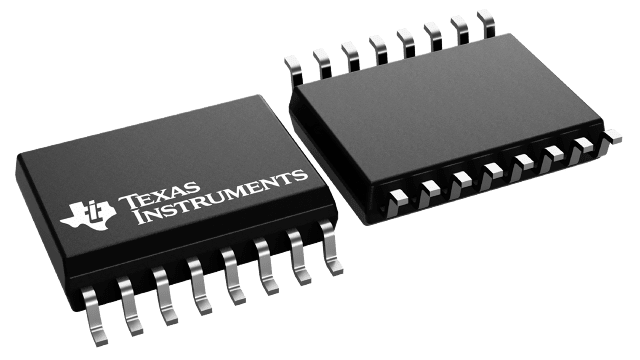
TLE2144IDWR
ActiveQUAD LOW-NOISE HIGH-SPEED PRECISION OPERATIONAL AMPLIFIER 16-SOIC -40 TO 105
Deep-Dive with AI
Search across all available documentation for this part.
TLE2144IDWR
ActiveQUAD LOW-NOISE HIGH-SPEED PRECISION OPERATIONAL AMPLIFIER 16-SOIC -40 TO 105
Deep-Dive with AI
Technical Specifications
Parameters and characteristics commom to parts in this series
| Specification | TLE2144IDWR | TLE2144 Series |
|---|---|---|
| Amplifier Type | General Purpose | General Purpose |
| Current - Input Bias | 700 nA | 700 nA |
| Current - Output / Channel | 50 mA | 50 mA |
| Current - Supply | 6.9 mA | 6.9 mA |
| Current - Supply | - | 13.8 mA |
| Gain Bandwidth Product | 5.9 MHz | 5.9 MHz |
| Mounting Type | Surface Mount | Surface Mount, Through Hole |
| Number of Circuits | 4 | 4 |
| Operating Temperature [Max] | 105 ░C | 70 - 125 ░C |
| Operating Temperature [Min] | -40 °C | -55 - 0 °C |
| Output Type | Rail-to-Rail | Rail-to-Rail |
| Package / Case | 16-SOIC | 16-SOIC, 14-DIP |
| Package / Case | - | 7.62 mm |
| Package / Case | - | 0.3 in |
| Slew Rate | 45 V/µs | 45 V/µs |
| Supplier Device Package | 16-SOIC | 16-SOIC |
| Voltage - Input Offset | 290 µV | 290 - 600 µV |
| Voltage - Supply Span (Max) [Max] | 44 V | 44 V |
| Voltage - Supply Span (Min) [Min] | 4 V | 4 V |
Pricing
Prices provided here are for design reference only. For realtime values and availability, please visit the distributors directly
TLE2144 Series
Enhanced Product Excaliber Low-Noise High-Speed Precision Quad Operational Amplifier
| Part | Operating Temperature [Max] | Operating Temperature [Min] | Voltage - Supply Span (Max) [Max] | Current - Input Bias | Voltage - Input Offset | Current - Output / Channel | Slew Rate | Output Type | Number of Circuits | Current - Supply | Gain Bandwidth Product | Supplier Device Package | Mounting Type | Package / Case | Amplifier Type | Voltage - Supply Span (Min) [Min] | Current - Supply [custom] | Package / Case | Package / Case |
|---|---|---|---|---|---|---|---|---|---|---|---|---|---|---|---|---|---|---|---|
Texas Instruments TLE2144CDWThe TLE214x and TLE214xA devices are high-performance, internally compensated operational amplifiers built using Texas Instruments complementary bipolar Excalibur process. The TLE214xA is a tighter offset voltage grade of the TLE214x. Both are pin-compatible upgrades to standard industry products.
The design incorporates an input stage that simultaneously achieves low audio-band noise of 10.5 nV//100-pF load is useful in fast actuator/positioning drivers. Under similar test conditions, settling time to 0.01% is 400 ns.
The devices are stable with capacitive loads up to 10 nF, although the 6-MHz bandwidth decreases to 1.8 MHz at this high loading level. As such, the TLE214x and TLE214xA are useful for low-droop sample-and-holds and direct buffering of long cables, including 4-mA to 20-mA current loops.
The special design also exhibits an improved insensitivity to inherent integrated circuit component mismatches as is evidenced by a 500-µV maximum offset voltage and 1.7-µV/°C typical drift. Minimum common-mode rejection ratio and supply-voltage rejection ratio are 85 dB and 90 dB, respectively.
Device performance is relatively independent of supply voltage over the ±2-V to ±22-V range. Inputs can operate between VCC–– 0.3 to VCC+– 1.8 V without inducing phase reversal, although excessive input current may flow out of each input exceeding the lower common-mode input range. The all-npn output stage provides a nearly rail-to-rail output swing of VCC–– 0.1 to VCC+– 1 V under light current-loading conditions. The device can sustain shorts to either supply since output current is internally limited, but care must be taken to ensure that maximum package power dissipation is not exceeded.
Both versions can also be used as comparators. Differential inputs of VCC±can be maintained without damage to the device. Open-loop propagation delay with TTL supply levels is typically 200 ns. This gives a good indication as to output stage saturation recovery when the device is driven beyond the limits of recommended output swing.
Both the TLE214x and TLE214xA are available in a wide variety of packages, including both the industry-standard 8-pin small-outline version and chip form for high-density system applications. The C-suffix devices are characterized for operation from 0°C to 70°C, I-suffix devices from –40°C to 105°C, and M-suffix devices over the full military temperature range of –55°C to 125°C.
The TLE214x and TLE214xA devices are high-performance, internally compensated operational amplifiers built using Texas Instruments complementary bipolar Excalibur process. The TLE214xA is a tighter offset voltage grade of the TLE214x. Both are pin-compatible upgrades to standard industry products.
The design incorporates an input stage that simultaneously achieves low audio-band noise of 10.5 nV//100-pF load is useful in fast actuator/positioning drivers. Under similar test conditions, settling time to 0.01% is 400 ns.
The devices are stable with capacitive loads up to 10 nF, although the 6-MHz bandwidth decreases to 1.8 MHz at this high loading level. As such, the TLE214x and TLE214xA are useful for low-droop sample-and-holds and direct buffering of long cables, including 4-mA to 20-mA current loops.
The special design also exhibits an improved insensitivity to inherent integrated circuit component mismatches as is evidenced by a 500-µV maximum offset voltage and 1.7-µV/°C typical drift. Minimum common-mode rejection ratio and supply-voltage rejection ratio are 85 dB and 90 dB, respectively.
Device performance is relatively independent of supply voltage over the ±2-V to ±22-V range. Inputs can operate between VCC–– 0.3 to VCC+– 1.8 V without inducing phase reversal, although excessive input current may flow out of each input exceeding the lower common-mode input range. The all-npn output stage provides a nearly rail-to-rail output swing of VCC–– 0.1 to VCC+– 1 V under light current-loading conditions. The device can sustain shorts to either supply since output current is internally limited, but care must be taken to ensure that maximum package power dissipation is not exceeded.
Both versions can also be used as comparators. Differential inputs of VCC±can be maintained without damage to the device. Open-loop propagation delay with TTL supply levels is typically 200 ns. This gives a good indication as to output stage saturation recovery when the device is driven beyond the limits of recommended output swing.
Both the TLE214x and TLE214xA are available in a wide variety of packages, including both the industry-standard 8-pin small-outline version and chip form for high-density system applications. The C-suffix devices are characterized for operation from 0°C to 70°C, I-suffix devices from –40°C to 105°C, and M-suffix devices over the full military temperature range of –55°C to 125°C. | 70 ░C | 0 °C | 44 V | 700 nA | 290 µV | 50 mA | 45 V/µs | Rail-to-Rail | 4 | 6.9 mA | 5.9 MHz | 16-SOIC | Surface Mount | 16-SOIC | General Purpose | 4 V | |||
Texas Instruments TLE2144IDWThe TLE214x and TLE214xA devices are high-performance, internally compensated operational amplifiers built using Texas Instruments complementary bipolar Excalibur process. The TLE214xA is a tighter offset voltage grade of the TLE214x. Both are pin-compatible upgrades to standard industry products.
The design incorporates an input stage that simultaneously achieves low audio-band noise of 10.5 nV//100-pF load is useful in fast actuator/positioning drivers. Under similar test conditions, settling time to 0.01% is 400 ns.
The devices are stable with capacitive loads up to 10 nF, although the 6-MHz bandwidth decreases to 1.8 MHz at this high loading level. As such, the TLE214x and TLE214xA are useful for low-droop sample-and-holds and direct buffering of long cables, including 4-mA to 20-mA current loops.
The special design also exhibits an improved insensitivity to inherent integrated circuit component mismatches as is evidenced by a 500-µV maximum offset voltage and 1.7-µV/°C typical drift. Minimum common-mode rejection ratio and supply-voltage rejection ratio are 85 dB and 90 dB, respectively.
Device performance is relatively independent of supply voltage over the ±2-V to ±22-V range. Inputs can operate between VCC–– 0.3 to VCC+– 1.8 V without inducing phase reversal, although excessive input current may flow out of each input exceeding the lower common-mode input range. The all-npn output stage provides a nearly rail-to-rail output swing of VCC–– 0.1 to VCC+– 1 V under light current-loading conditions. The device can sustain shorts to either supply since output current is internally limited, but care must be taken to ensure that maximum package power dissipation is not exceeded.
Both versions can also be used as comparators. Differential inputs of VCC±can be maintained without damage to the device. Open-loop propagation delay with TTL supply levels is typically 200 ns. This gives a good indication as to output stage saturation recovery when the device is driven beyond the limits of recommended output swing.
Both the TLE214x and TLE214xA are available in a wide variety of packages, including both the industry-standard 8-pin small-outline version and chip form for high-density system applications. The C-suffix devices are characterized for operation from 0°C to 70°C, I-suffix devices from –40°C to 105°C, and M-suffix devices over the full military temperature range of –55°C to 125°C.
The TLE214x and TLE214xA devices are high-performance, internally compensated operational amplifiers built using Texas Instruments complementary bipolar Excalibur process. The TLE214xA is a tighter offset voltage grade of the TLE214x. Both are pin-compatible upgrades to standard industry products.
The design incorporates an input stage that simultaneously achieves low audio-band noise of 10.5 nV//100-pF load is useful in fast actuator/positioning drivers. Under similar test conditions, settling time to 0.01% is 400 ns.
The devices are stable with capacitive loads up to 10 nF, although the 6-MHz bandwidth decreases to 1.8 MHz at this high loading level. As such, the TLE214x and TLE214xA are useful for low-droop sample-and-holds and direct buffering of long cables, including 4-mA to 20-mA current loops.
The special design also exhibits an improved insensitivity to inherent integrated circuit component mismatches as is evidenced by a 500-µV maximum offset voltage and 1.7-µV/°C typical drift. Minimum common-mode rejection ratio and supply-voltage rejection ratio are 85 dB and 90 dB, respectively.
Device performance is relatively independent of supply voltage over the ±2-V to ±22-V range. Inputs can operate between VCC–– 0.3 to VCC+– 1.8 V without inducing phase reversal, although excessive input current may flow out of each input exceeding the lower common-mode input range. The all-npn output stage provides a nearly rail-to-rail output swing of VCC–– 0.1 to VCC+– 1 V under light current-loading conditions. The device can sustain shorts to either supply since output current is internally limited, but care must be taken to ensure that maximum package power dissipation is not exceeded.
Both versions can also be used as comparators. Differential inputs of VCC±can be maintained without damage to the device. Open-loop propagation delay with TTL supply levels is typically 200 ns. This gives a good indication as to output stage saturation recovery when the device is driven beyond the limits of recommended output swing.
Both the TLE214x and TLE214xA are available in a wide variety of packages, including both the industry-standard 8-pin small-outline version and chip form for high-density system applications. The C-suffix devices are characterized for operation from 0°C to 70°C, I-suffix devices from –40°C to 105°C, and M-suffix devices over the full military temperature range of –55°C to 125°C. | 105 ░C | -40 °C | 44 V | 700 nA | 290 µV | 50 mA | 45 V/µs | Rail-to-Rail | 4 | 6.9 mA | 5.9 MHz | 16-SOIC | Surface Mount | 16-SOIC | General Purpose | 4 V | |||
Texas Instruments TLE2144MDWREPThe TLE214x devices are high-performance, internally compensated operational amplifiers built using the Texas Instruments complementary bipolar Excalibur. process. They are pin-compatible upgrades to standard industry products.
The design incorporates an input stage that simultaneously achieves low audio-band noise of 10.5 nV//100-pF load is useful in fast actuator/positioning drivers. Under similar test conditions, settling time to 0.01% is 400 ns.
The devices are stable with capacitive loads up to 10 nF, although the 6-MHz bandwidth decreases to 1.8 MHz at this high loading level. As such, the TLE214x are useful for low-droop sample-and-holds and direct buffering of long cables, including 4-mA to 20-mA current loops.
The special design also exhibits an improved insensitivity to inherent integrated circuit component mismatches as is evidenced by a 900-µV maximum offset voltage and 1.7-µV/°C typical drift. Minimum common-mode rejection ratio and supply-voltage rejection ratio are 85 dB and 90 dB, respectively.
Device performance is relatively independent of supply voltage over the ±2-V to ±22-V range. Inputs can operate between VCC–– 0.3 V to VCC+– 1.8 V without inducing phase reversal, although excessive input current may flow out of each input exceeding the lower common-mode input range. The all-npn output stage provides a nearly rail-to-rail output swing of VCC–– 0.1 V to VCC+– 1 V under light current-loading conditions. The device can sustain shorts to either supply since output current is internally limited, but care must be taken to ensure that maximum package power dissipation is not exceeded.
Both versions can also be used as comparators. Differential inputs of VCC±can be maintained without damage to the device. Open-loop propagation delay with TTL supply levels is typically 200 ns. This gives a good indication as to output stage saturation recovery when the device is driven beyond the limits of recommended output swing.
The TLE214x devices are available in industry-standard 8-pin and 16-pin small-outline packages. The devices are characterized for operation from –55°C to 125°C.
The TLE214x devices are high-performance, internally compensated operational amplifiers built using the Texas Instruments complementary bipolar Excalibur. process. They are pin-compatible upgrades to standard industry products.
The design incorporates an input stage that simultaneously achieves low audio-band noise of 10.5 nV//100-pF load is useful in fast actuator/positioning drivers. Under similar test conditions, settling time to 0.01% is 400 ns.
The devices are stable with capacitive loads up to 10 nF, although the 6-MHz bandwidth decreases to 1.8 MHz at this high loading level. As such, the TLE214x are useful for low-droop sample-and-holds and direct buffering of long cables, including 4-mA to 20-mA current loops.
The special design also exhibits an improved insensitivity to inherent integrated circuit component mismatches as is evidenced by a 900-µV maximum offset voltage and 1.7-µV/°C typical drift. Minimum common-mode rejection ratio and supply-voltage rejection ratio are 85 dB and 90 dB, respectively.
Device performance is relatively independent of supply voltage over the ±2-V to ±22-V range. Inputs can operate between VCC–– 0.3 V to VCC+– 1.8 V without inducing phase reversal, although excessive input current may flow out of each input exceeding the lower common-mode input range. The all-npn output stage provides a nearly rail-to-rail output swing of VCC–– 0.1 V to VCC+– 1 V under light current-loading conditions. The device can sustain shorts to either supply since output current is internally limited, but care must be taken to ensure that maximum package power dissipation is not exceeded.
Both versions can also be used as comparators. Differential inputs of VCC±can be maintained without damage to the device. Open-loop propagation delay with TTL supply levels is typically 200 ns. This gives a good indication as to output stage saturation recovery when the device is driven beyond the limits of recommended output swing.
The TLE214x devices are available in industry-standard 8-pin and 16-pin small-outline packages. The devices are characterized for operation from –55°C to 125°C. | 125 °C | -55 °C | 44 V | 700 nA | 600 µV | 50 mA | 45 V/µs | Rail-to-Rail | 4 | 5.9 MHz | 16-SOIC | Surface Mount | 16-SOIC | General Purpose | 4 V | 13.8 mA | |||
Texas Instruments TLE2144CNThe TLE214x and TLE214xA devices are high-performance, internally compensated operational amplifiers built using Texas Instruments complementary bipolar Excalibur process. The TLE214xA is a tighter offset voltage grade of the TLE214x. Both are pin-compatible upgrades to standard industry products.
The design incorporates an input stage that simultaneously achieves low audio-band noise of 10.5 nV//100-pF load is useful in fast actuator/positioning drivers. Under similar test conditions, settling time to 0.01% is 400 ns.
The devices are stable with capacitive loads up to 10 nF, although the 6-MHz bandwidth decreases to 1.8 MHz at this high loading level. As such, the TLE214x and TLE214xA are useful for low-droop sample-and-holds and direct buffering of long cables, including 4-mA to 20-mA current loops.
The special design also exhibits an improved insensitivity to inherent integrated circuit component mismatches as is evidenced by a 500-µV maximum offset voltage and 1.7-µV/°C typical drift. Minimum common-mode rejection ratio and supply-voltage rejection ratio are 85 dB and 90 dB, respectively.
Device performance is relatively independent of supply voltage over the ±2-V to ±22-V range. Inputs can operate between VCC–– 0.3 to VCC+– 1.8 V without inducing phase reversal, although excessive input current may flow out of each input exceeding the lower common-mode input range. The all-npn output stage provides a nearly rail-to-rail output swing of VCC–– 0.1 to VCC+– 1 V under light current-loading conditions. The device can sustain shorts to either supply since output current is internally limited, but care must be taken to ensure that maximum package power dissipation is not exceeded.
Both versions can also be used as comparators. Differential inputs of VCC±can be maintained without damage to the device. Open-loop propagation delay with TTL supply levels is typically 200 ns. This gives a good indication as to output stage saturation recovery when the device is driven beyond the limits of recommended output swing.
Both the TLE214x and TLE214xA are available in a wide variety of packages, including both the industry-standard 8-pin small-outline version and chip form for high-density system applications. The C-suffix devices are characterized for operation from 0°C to 70°C, I-suffix devices from –40°C to 105°C, and M-suffix devices over the full military temperature range of –55°C to 125°C.
The TLE214x and TLE214xA devices are high-performance, internally compensated operational amplifiers built using Texas Instruments complementary bipolar Excalibur process. The TLE214xA is a tighter offset voltage grade of the TLE214x. Both are pin-compatible upgrades to standard industry products.
The design incorporates an input stage that simultaneously achieves low audio-band noise of 10.5 nV//100-pF load is useful in fast actuator/positioning drivers. Under similar test conditions, settling time to 0.01% is 400 ns.
The devices are stable with capacitive loads up to 10 nF, although the 6-MHz bandwidth decreases to 1.8 MHz at this high loading level. As such, the TLE214x and TLE214xA are useful for low-droop sample-and-holds and direct buffering of long cables, including 4-mA to 20-mA current loops.
The special design also exhibits an improved insensitivity to inherent integrated circuit component mismatches as is evidenced by a 500-µV maximum offset voltage and 1.7-µV/°C typical drift. Minimum common-mode rejection ratio and supply-voltage rejection ratio are 85 dB and 90 dB, respectively.
Device performance is relatively independent of supply voltage over the ±2-V to ±22-V range. Inputs can operate between VCC–– 0.3 to VCC+– 1.8 V without inducing phase reversal, although excessive input current may flow out of each input exceeding the lower common-mode input range. The all-npn output stage provides a nearly rail-to-rail output swing of VCC–– 0.1 to VCC+– 1 V under light current-loading conditions. The device can sustain shorts to either supply since output current is internally limited, but care must be taken to ensure that maximum package power dissipation is not exceeded.
Both versions can also be used as comparators. Differential inputs of VCC±can be maintained without damage to the device. Open-loop propagation delay with TTL supply levels is typically 200 ns. This gives a good indication as to output stage saturation recovery when the device is driven beyond the limits of recommended output swing.
Both the TLE214x and TLE214xA are available in a wide variety of packages, including both the industry-standard 8-pin small-outline version and chip form for high-density system applications. The C-suffix devices are characterized for operation from 0°C to 70°C, I-suffix devices from –40°C to 105°C, and M-suffix devices over the full military temperature range of –55°C to 125°C. | 70 ░C | 0 °C | 44 V | 700 nA | 290 µV | 50 mA | 45 V/µs | Rail-to-Rail | 4 | 6.9 mA | 5.9 MHz | Through Hole | 14-DIP | General Purpose | 4 V | 7.62 mm | 0.3 in | ||
Texas Instruments TLE2144MDWThe TLE214x and TLE214xA devices are high-performance, internally compensated operational amplifiers built using Texas Instruments complementary bipolar Excalibur process. The TLE214xA is a tighter offset voltage grade of the TLE214x. Both are pin-compatible upgrades to standard industry products.
The design incorporates an input stage that simultaneously achieves low audio-band noise of 10.5 nV//100-pF load is useful in fast actuator/positioning drivers. Under similar test conditions, settling time to 0.01% is 400 ns.
The devices are stable with capacitive loads up to 10 nF, although the 6-MHz bandwidth decreases to 1.8 MHz at this high loading level. As such, the TLE214x and TLE214xA are useful for low-droop sample-and-holds and direct buffering of long cables, including 4-mA to 20-mA current loops.
The special design also exhibits an improved insensitivity to inherent integrated circuit component mismatches as is evidenced by a 500-µV maximum offset voltage and 1.7-µV/°C typical drift. Minimum common-mode rejection ratio and supply-voltage rejection ratio are 85 dB and 90 dB, respectively.
Device performance is relatively independent of supply voltage over the ±2-V to ±22-V range. Inputs can operate between VCC–– 0.3 to VCC+– 1.8 V without inducing phase reversal, although excessive input current may flow out of each input exceeding the lower common-mode input range. The all-npn output stage provides a nearly rail-to-rail output swing of VCC–– 0.1 to VCC+– 1 V under light current-loading conditions. The device can sustain shorts to either supply since output current is internally limited, but care must be taken to ensure that maximum package power dissipation is not exceeded.
Both versions can also be used as comparators. Differential inputs of VCC±can be maintained without damage to the device. Open-loop propagation delay with TTL supply levels is typically 200 ns. This gives a good indication as to output stage saturation recovery when the device is driven beyond the limits of recommended output swing.
Both the TLE214x and TLE214xA are available in a wide variety of packages, including both the industry-standard 8-pin small-outline version and chip form for high-density system applications. The C-suffix devices are characterized for operation from 0°C to 70°C, I-suffix devices from –40°C to 105°C, and M-suffix devices over the full military temperature range of –55°C to 125°C.
The TLE214x and TLE214xA devices are high-performance, internally compensated operational amplifiers built using Texas Instruments complementary bipolar Excalibur process. The TLE214xA is a tighter offset voltage grade of the TLE214x. Both are pin-compatible upgrades to standard industry products.
The design incorporates an input stage that simultaneously achieves low audio-band noise of 10.5 nV//100-pF load is useful in fast actuator/positioning drivers. Under similar test conditions, settling time to 0.01% is 400 ns.
The devices are stable with capacitive loads up to 10 nF, although the 6-MHz bandwidth decreases to 1.8 MHz at this high loading level. As such, the TLE214x and TLE214xA are useful for low-droop sample-and-holds and direct buffering of long cables, including 4-mA to 20-mA current loops.
The special design also exhibits an improved insensitivity to inherent integrated circuit component mismatches as is evidenced by a 500-µV maximum offset voltage and 1.7-µV/°C typical drift. Minimum common-mode rejection ratio and supply-voltage rejection ratio are 85 dB and 90 dB, respectively.
Device performance is relatively independent of supply voltage over the ±2-V to ±22-V range. Inputs can operate between VCC–– 0.3 to VCC+– 1.8 V without inducing phase reversal, although excessive input current may flow out of each input exceeding the lower common-mode input range. The all-npn output stage provides a nearly rail-to-rail output swing of VCC–– 0.1 to VCC+– 1 V under light current-loading conditions. The device can sustain shorts to either supply since output current is internally limited, but care must be taken to ensure that maximum package power dissipation is not exceeded.
Both versions can also be used as comparators. Differential inputs of VCC±can be maintained without damage to the device. Open-loop propagation delay with TTL supply levels is typically 200 ns. This gives a good indication as to output stage saturation recovery when the device is driven beyond the limits of recommended output swing.
Both the TLE214x and TLE214xA are available in a wide variety of packages, including both the industry-standard 8-pin small-outline version and chip form for high-density system applications. The C-suffix devices are characterized for operation from 0°C to 70°C, I-suffix devices from –40°C to 105°C, and M-suffix devices over the full military temperature range of –55°C to 125°C. | 125 °C | -55 °C | 44 V | 700 nA | 290 µV | 50 mA | 45 V/µs | Rail-to-Rail | 4 | 6.9 mA | 5.9 MHz | 16-SOIC | Surface Mount | 16-SOIC | General Purpose | 4 V | |||
Texas Instruments TLE2144ACNThe TLE214x and TLE214xA devices are high-performance, internally compensated operational amplifiers built using Texas Instruments complementary bipolar Excalibur process. The TLE214xA is a tighter offset voltage grade of the TLE214x. Both are pin-compatible upgrades to standard industry products.
The design incorporates an input stage that simultaneously achieves low audio-band noise of 10.5 nV//100-pF load is useful in fast actuator/positioning drivers. Under similar test conditions, settling time to 0.01% is 400 ns.
The devices are stable with capacitive loads up to 10 nF, although the 6-MHz bandwidth decreases to 1.8 MHz at this high loading level. As such, the TLE214x and TLE214xA are useful for low-droop sample-and-holds and direct buffering of long cables, including 4-mA to 20-mA current loops.
The special design also exhibits an improved insensitivity to inherent integrated circuit component mismatches as is evidenced by a 500-µV maximum offset voltage and 1.7-µV/°C typical drift. Minimum common-mode rejection ratio and supply-voltage rejection ratio are 85 dB and 90 dB, respectively.
Device performance is relatively independent of supply voltage over the ±2-V to ±22-V range. Inputs can operate between VCC–– 0.3 to VCC+– 1.8 V without inducing phase reversal, although excessive input current may flow out of each input exceeding the lower common-mode input range. The all-npn output stage provides a nearly rail-to-rail output swing of VCC–– 0.1 to VCC+– 1 V under light current-loading conditions. The device can sustain shorts to either supply since output current is internally limited, but care must be taken to ensure that maximum package power dissipation is not exceeded.
Both versions can also be used as comparators. Differential inputs of VCC±can be maintained without damage to the device. Open-loop propagation delay with TTL supply levels is typically 200 ns. This gives a good indication as to output stage saturation recovery when the device is driven beyond the limits of recommended output swing.
Both the TLE214x and TLE214xA are available in a wide variety of packages, including both the industry-standard 8-pin small-outline version and chip form for high-density system applications. The C-suffix devices are characterized for operation from 0°C to 70°C, I-suffix devices from –40°C to 105°C, and M-suffix devices over the full military temperature range of –55°C to 125°C.
The TLE214x and TLE214xA devices are high-performance, internally compensated operational amplifiers built using Texas Instruments complementary bipolar Excalibur process. The TLE214xA is a tighter offset voltage grade of the TLE214x. Both are pin-compatible upgrades to standard industry products.
The design incorporates an input stage that simultaneously achieves low audio-band noise of 10.5 nV//100-pF load is useful in fast actuator/positioning drivers. Under similar test conditions, settling time to 0.01% is 400 ns.
The devices are stable with capacitive loads up to 10 nF, although the 6-MHz bandwidth decreases to 1.8 MHz at this high loading level. As such, the TLE214x and TLE214xA are useful for low-droop sample-and-holds and direct buffering of long cables, including 4-mA to 20-mA current loops.
The special design also exhibits an improved insensitivity to inherent integrated circuit component mismatches as is evidenced by a 500-µV maximum offset voltage and 1.7-µV/°C typical drift. Minimum common-mode rejection ratio and supply-voltage rejection ratio are 85 dB and 90 dB, respectively.
Device performance is relatively independent of supply voltage over the ±2-V to ±22-V range. Inputs can operate between VCC–– 0.3 to VCC+– 1.8 V without inducing phase reversal, although excessive input current may flow out of each input exceeding the lower common-mode input range. The all-npn output stage provides a nearly rail-to-rail output swing of VCC–– 0.1 to VCC+– 1 V under light current-loading conditions. The device can sustain shorts to either supply since output current is internally limited, but care must be taken to ensure that maximum package power dissipation is not exceeded.
Both versions can also be used as comparators. Differential inputs of VCC±can be maintained without damage to the device. Open-loop propagation delay with TTL supply levels is typically 200 ns. This gives a good indication as to output stage saturation recovery when the device is driven beyond the limits of recommended output swing.
Both the TLE214x and TLE214xA are available in a wide variety of packages, including both the industry-standard 8-pin small-outline version and chip form for high-density system applications. The C-suffix devices are characterized for operation from 0°C to 70°C, I-suffix devices from –40°C to 105°C, and M-suffix devices over the full military temperature range of –55°C to 125°C. | 70 ░C | 0 °C | 44 V | 700 nA | 500 çV | 50 mA | 45 V/µs | Rail-to-Rail | 4 | 5.9 MHz | Through Hole | 14-DIP | General Purpose | 4 V | 13.8 mA | 7.62 mm | 0.3 in | ||
Texas Instruments TLE2144MDWG4The TLE214x and TLE214xA devices are high-performance, internally compensated operational amplifiers built using Texas Instruments complementary bipolar Excalibur process. The TLE214xA is a tighter offset voltage grade of the TLE214x. Both are pin-compatible upgrades to standard industry products.
The design incorporates an input stage that simultaneously achieves low audio-band noise of 10.5 nV//100-pF load is useful in fast actuator/positioning drivers. Under similar test conditions, settling time to 0.01% is 400 ns.
The devices are stable with capacitive loads up to 10 nF, although the 6-MHz bandwidth decreases to 1.8 MHz at this high loading level. As such, the TLE214x and TLE214xA are useful for low-droop sample-and-holds and direct buffering of long cables, including 4-mA to 20-mA current loops.
The special design also exhibits an improved insensitivity to inherent integrated circuit component mismatches as is evidenced by a 500-µV maximum offset voltage and 1.7-µV/°C typical drift. Minimum common-mode rejection ratio and supply-voltage rejection ratio are 85 dB and 90 dB, respectively.
Device performance is relatively independent of supply voltage over the ±2-V to ±22-V range. Inputs can operate between VCC–– 0.3 to VCC+– 1.8 V without inducing phase reversal, although excessive input current may flow out of each input exceeding the lower common-mode input range. The all-npn output stage provides a nearly rail-to-rail output swing of VCC–– 0.1 to VCC+– 1 V under light current-loading conditions. The device can sustain shorts to either supply since output current is internally limited, but care must be taken to ensure that maximum package power dissipation is not exceeded.
Both versions can also be used as comparators. Differential inputs of VCC±can be maintained without damage to the device. Open-loop propagation delay with TTL supply levels is typically 200 ns. This gives a good indication as to output stage saturation recovery when the device is driven beyond the limits of recommended output swing.
Both the TLE214x and TLE214xA are available in a wide variety of packages, including both the industry-standard 8-pin small-outline version and chip form for high-density system applications. The C-suffix devices are characterized for operation from 0°C to 70°C, I-suffix devices from –40°C to 105°C, and M-suffix devices over the full military temperature range of –55°C to 125°C.
The TLE214x and TLE214xA devices are high-performance, internally compensated operational amplifiers built using Texas Instruments complementary bipolar Excalibur process. The TLE214xA is a tighter offset voltage grade of the TLE214x. Both are pin-compatible upgrades to standard industry products.
The design incorporates an input stage that simultaneously achieves low audio-band noise of 10.5 nV//100-pF load is useful in fast actuator/positioning drivers. Under similar test conditions, settling time to 0.01% is 400 ns.
The devices are stable with capacitive loads up to 10 nF, although the 6-MHz bandwidth decreases to 1.8 MHz at this high loading level. As such, the TLE214x and TLE214xA are useful for low-droop sample-and-holds and direct buffering of long cables, including 4-mA to 20-mA current loops.
The special design also exhibits an improved insensitivity to inherent integrated circuit component mismatches as is evidenced by a 500-µV maximum offset voltage and 1.7-µV/°C typical drift. Minimum common-mode rejection ratio and supply-voltage rejection ratio are 85 dB and 90 dB, respectively.
Device performance is relatively independent of supply voltage over the ±2-V to ±22-V range. Inputs can operate between VCC–– 0.3 to VCC+– 1.8 V without inducing phase reversal, although excessive input current may flow out of each input exceeding the lower common-mode input range. The all-npn output stage provides a nearly rail-to-rail output swing of VCC–– 0.1 to VCC+– 1 V under light current-loading conditions. The device can sustain shorts to either supply since output current is internally limited, but care must be taken to ensure that maximum package power dissipation is not exceeded.
Both versions can also be used as comparators. Differential inputs of VCC±can be maintained without damage to the device. Open-loop propagation delay with TTL supply levels is typically 200 ns. This gives a good indication as to output stage saturation recovery when the device is driven beyond the limits of recommended output swing.
Both the TLE214x and TLE214xA are available in a wide variety of packages, including both the industry-standard 8-pin small-outline version and chip form for high-density system applications. The C-suffix devices are characterized for operation from 0°C to 70°C, I-suffix devices from –40°C to 105°C, and M-suffix devices over the full military temperature range of –55°C to 125°C. | 125 °C | -55 °C | 44 V | 700 nA | 290 µV | 50 mA | 45 V/µs | Rail-to-Rail | 4 | 6.9 mA | 5.9 MHz | 16-SOIC | Surface Mount | 16-SOIC | General Purpose | 4 V | |||
70 ░C | 0 °C | 44 V | 700 nA | 290 µV | 50 mA | 45 V/µs | Rail-to-Rail | 4 | 6.9 mA | 5.9 MHz | 16-SOIC | Surface Mount | 16-SOIC | General Purpose | 4 V | ||||
Texas Instruments TLE2144IDWRThe TLE214x and TLE214xA devices are high-performance, internally compensated operational amplifiers built using Texas Instruments complementary bipolar Excalibur process. The TLE214xA is a tighter offset voltage grade of the TLE214x. Both are pin-compatible upgrades to standard industry products.
The design incorporates an input stage that simultaneously achieves low audio-band noise of 10.5 nV//100-pF load is useful in fast actuator/positioning drivers. Under similar test conditions, settling time to 0.01% is 400 ns.
The devices are stable with capacitive loads up to 10 nF, although the 6-MHz bandwidth decreases to 1.8 MHz at this high loading level. As such, the TLE214x and TLE214xA are useful for low-droop sample-and-holds and direct buffering of long cables, including 4-mA to 20-mA current loops.
The special design also exhibits an improved insensitivity to inherent integrated circuit component mismatches as is evidenced by a 500-µV maximum offset voltage and 1.7-µV/°C typical drift. Minimum common-mode rejection ratio and supply-voltage rejection ratio are 85 dB and 90 dB, respectively.
Device performance is relatively independent of supply voltage over the ±2-V to ±22-V range. Inputs can operate between VCC–– 0.3 to VCC+– 1.8 V without inducing phase reversal, although excessive input current may flow out of each input exceeding the lower common-mode input range. The all-npn output stage provides a nearly rail-to-rail output swing of VCC–– 0.1 to VCC+– 1 V under light current-loading conditions. The device can sustain shorts to either supply since output current is internally limited, but care must be taken to ensure that maximum package power dissipation is not exceeded.
Both versions can also be used as comparators. Differential inputs of VCC±can be maintained without damage to the device. Open-loop propagation delay with TTL supply levels is typically 200 ns. This gives a good indication as to output stage saturation recovery when the device is driven beyond the limits of recommended output swing.
Both the TLE214x and TLE214xA are available in a wide variety of packages, including both the industry-standard 8-pin small-outline version and chip form for high-density system applications. The C-suffix devices are characterized for operation from 0°C to 70°C, I-suffix devices from –40°C to 105°C, and M-suffix devices over the full military temperature range of –55°C to 125°C.
The TLE214x and TLE214xA devices are high-performance, internally compensated operational amplifiers built using Texas Instruments complementary bipolar Excalibur process. The TLE214xA is a tighter offset voltage grade of the TLE214x. Both are pin-compatible upgrades to standard industry products.
The design incorporates an input stage that simultaneously achieves low audio-band noise of 10.5 nV//100-pF load is useful in fast actuator/positioning drivers. Under similar test conditions, settling time to 0.01% is 400 ns.
The devices are stable with capacitive loads up to 10 nF, although the 6-MHz bandwidth decreases to 1.8 MHz at this high loading level. As such, the TLE214x and TLE214xA are useful for low-droop sample-and-holds and direct buffering of long cables, including 4-mA to 20-mA current loops.
The special design also exhibits an improved insensitivity to inherent integrated circuit component mismatches as is evidenced by a 500-µV maximum offset voltage and 1.7-µV/°C typical drift. Minimum common-mode rejection ratio and supply-voltage rejection ratio are 85 dB and 90 dB, respectively.
Device performance is relatively independent of supply voltage over the ±2-V to ±22-V range. Inputs can operate between VCC–– 0.3 to VCC+– 1.8 V without inducing phase reversal, although excessive input current may flow out of each input exceeding the lower common-mode input range. The all-npn output stage provides a nearly rail-to-rail output swing of VCC–– 0.1 to VCC+– 1 V under light current-loading conditions. The device can sustain shorts to either supply since output current is internally limited, but care must be taken to ensure that maximum package power dissipation is not exceeded.
Both versions can also be used as comparators. Differential inputs of VCC±can be maintained without damage to the device. Open-loop propagation delay with TTL supply levels is typically 200 ns. This gives a good indication as to output stage saturation recovery when the device is driven beyond the limits of recommended output swing.
Both the TLE214x and TLE214xA are available in a wide variety of packages, including both the industry-standard 8-pin small-outline version and chip form for high-density system applications. The C-suffix devices are characterized for operation from 0°C to 70°C, I-suffix devices from –40°C to 105°C, and M-suffix devices over the full military temperature range of –55°C to 125°C. | 105 ░C | -40 °C | 44 V | 700 nA | 290 µV | 50 mA | 45 V/µs | Rail-to-Rail | 4 | 6.9 mA | 5.9 MHz | 16-SOIC | Surface Mount | 16-SOIC | General Purpose | 4 V | |||
Texas Instruments TLE2144AINThe TLE214x and TLE214xA devices are high-performance, internally compensated operational amplifiers built using Texas Instruments complementary bipolar Excalibur process. The TLE214xA is a tighter offset voltage grade of the TLE214x. Both are pin-compatible upgrades to standard industry products.
The design incorporates an input stage that simultaneously achieves low audio-band noise of 10.5 nV//100-pF load is useful in fast actuator/positioning drivers. Under similar test conditions, settling time to 0.01% is 400 ns.
The devices are stable with capacitive loads up to 10 nF, although the 6-MHz bandwidth decreases to 1.8 MHz at this high loading level. As such, the TLE214x and TLE214xA are useful for low-droop sample-and-holds and direct buffering of long cables, including 4-mA to 20-mA current loops.
The special design also exhibits an improved insensitivity to inherent integrated circuit component mismatches as is evidenced by a 500-µV maximum offset voltage and 1.7-µV/°C typical drift. Minimum common-mode rejection ratio and supply-voltage rejection ratio are 85 dB and 90 dB, respectively.
Device performance is relatively independent of supply voltage over the ±2-V to ±22-V range. Inputs can operate between VCC–– 0.3 to VCC+– 1.8 V without inducing phase reversal, although excessive input current may flow out of each input exceeding the lower common-mode input range. The all-npn output stage provides a nearly rail-to-rail output swing of VCC–– 0.1 to VCC+– 1 V under light current-loading conditions. The device can sustain shorts to either supply since output current is internally limited, but care must be taken to ensure that maximum package power dissipation is not exceeded.
Both versions can also be used as comparators. Differential inputs of VCC±can be maintained without damage to the device. Open-loop propagation delay with TTL supply levels is typically 200 ns. This gives a good indication as to output stage saturation recovery when the device is driven beyond the limits of recommended output swing.
Both the TLE214x and TLE214xA are available in a wide variety of packages, including both the industry-standard 8-pin small-outline version and chip form for high-density system applications. The C-suffix devices are characterized for operation from 0°C to 70°C, I-suffix devices from –40°C to 105°C, and M-suffix devices over the full military temperature range of –55°C to 125°C.
The TLE214x and TLE214xA devices are high-performance, internally compensated operational amplifiers built using Texas Instruments complementary bipolar Excalibur process. The TLE214xA is a tighter offset voltage grade of the TLE214x. Both are pin-compatible upgrades to standard industry products.
The design incorporates an input stage that simultaneously achieves low audio-band noise of 10.5 nV//100-pF load is useful in fast actuator/positioning drivers. Under similar test conditions, settling time to 0.01% is 400 ns.
The devices are stable with capacitive loads up to 10 nF, although the 6-MHz bandwidth decreases to 1.8 MHz at this high loading level. As such, the TLE214x and TLE214xA are useful for low-droop sample-and-holds and direct buffering of long cables, including 4-mA to 20-mA current loops.
The special design also exhibits an improved insensitivity to inherent integrated circuit component mismatches as is evidenced by a 500-µV maximum offset voltage and 1.7-µV/°C typical drift. Minimum common-mode rejection ratio and supply-voltage rejection ratio are 85 dB and 90 dB, respectively.
Device performance is relatively independent of supply voltage over the ±2-V to ±22-V range. Inputs can operate between VCC–– 0.3 to VCC+– 1.8 V without inducing phase reversal, although excessive input current may flow out of each input exceeding the lower common-mode input range. The all-npn output stage provides a nearly rail-to-rail output swing of VCC–– 0.1 to VCC+– 1 V under light current-loading conditions. The device can sustain shorts to either supply since output current is internally limited, but care must be taken to ensure that maximum package power dissipation is not exceeded.
Both versions can also be used as comparators. Differential inputs of VCC±can be maintained without damage to the device. Open-loop propagation delay with TTL supply levels is typically 200 ns. This gives a good indication as to output stage saturation recovery when the device is driven beyond the limits of recommended output swing.
Both the TLE214x and TLE214xA are available in a wide variety of packages, including both the industry-standard 8-pin small-outline version and chip form for high-density system applications. The C-suffix devices are characterized for operation from 0°C to 70°C, I-suffix devices from –40°C to 105°C, and M-suffix devices over the full military temperature range of –55°C to 125°C. | 105 ░C | -40 °C | 44 V | 700 nA | 290 µV | 50 mA | 45 V/µs | Rail-to-Rail | 4 | 6.9 mA | 5.9 MHz | Through Hole | 14-DIP | General Purpose | 4 V | 7.62 mm | 0.3 in | ||
Texas Instruments TLE2144CDWRThe TLE214x and TLE214xA devices are high-performance, internally compensated operational amplifiers built using Texas Instruments complementary bipolar Excalibur process. The TLE214xA is a tighter offset voltage grade of the TLE214x. Both are pin-compatible upgrades to standard industry products.
The design incorporates an input stage that simultaneously achieves low audio-band noise of 10.5 nV//100-pF load is useful in fast actuator/positioning drivers. Under similar test conditions, settling time to 0.01% is 400 ns.
The devices are stable with capacitive loads up to 10 nF, although the 6-MHz bandwidth decreases to 1.8 MHz at this high loading level. As such, the TLE214x and TLE214xA are useful for low-droop sample-and-holds and direct buffering of long cables, including 4-mA to 20-mA current loops.
The special design also exhibits an improved insensitivity to inherent integrated circuit component mismatches as is evidenced by a 500-µV maximum offset voltage and 1.7-µV/°C typical drift. Minimum common-mode rejection ratio and supply-voltage rejection ratio are 85 dB and 90 dB, respectively.
Device performance is relatively independent of supply voltage over the ±2-V to ±22-V range. Inputs can operate between VCC–– 0.3 to VCC+– 1.8 V without inducing phase reversal, although excessive input current may flow out of each input exceeding the lower common-mode input range. The all-npn output stage provides a nearly rail-to-rail output swing of VCC–– 0.1 to VCC+– 1 V under light current-loading conditions. The device can sustain shorts to either supply since output current is internally limited, but care must be taken to ensure that maximum package power dissipation is not exceeded.
Both versions can also be used as comparators. Differential inputs of VCC±can be maintained without damage to the device. Open-loop propagation delay with TTL supply levels is typically 200 ns. This gives a good indication as to output stage saturation recovery when the device is driven beyond the limits of recommended output swing.
Both the TLE214x and TLE214xA are available in a wide variety of packages, including both the industry-standard 8-pin small-outline version and chip form for high-density system applications. The C-suffix devices are characterized for operation from 0°C to 70°C, I-suffix devices from –40°C to 105°C, and M-suffix devices over the full military temperature range of –55°C to 125°C.
The TLE214x and TLE214xA devices are high-performance, internally compensated operational amplifiers built using Texas Instruments complementary bipolar Excalibur process. The TLE214xA is a tighter offset voltage grade of the TLE214x. Both are pin-compatible upgrades to standard industry products.
The design incorporates an input stage that simultaneously achieves low audio-band noise of 10.5 nV//100-pF load is useful in fast actuator/positioning drivers. Under similar test conditions, settling time to 0.01% is 400 ns.
The devices are stable with capacitive loads up to 10 nF, although the 6-MHz bandwidth decreases to 1.8 MHz at this high loading level. As such, the TLE214x and TLE214xA are useful for low-droop sample-and-holds and direct buffering of long cables, including 4-mA to 20-mA current loops.
The special design also exhibits an improved insensitivity to inherent integrated circuit component mismatches as is evidenced by a 500-µV maximum offset voltage and 1.7-µV/°C typical drift. Minimum common-mode rejection ratio and supply-voltage rejection ratio are 85 dB and 90 dB, respectively.
Device performance is relatively independent of supply voltage over the ±2-V to ±22-V range. Inputs can operate between VCC–– 0.3 to VCC+– 1.8 V without inducing phase reversal, although excessive input current may flow out of each input exceeding the lower common-mode input range. The all-npn output stage provides a nearly rail-to-rail output swing of VCC–– 0.1 to VCC+– 1 V under light current-loading conditions. The device can sustain shorts to either supply since output current is internally limited, but care must be taken to ensure that maximum package power dissipation is not exceeded.
Both versions can also be used as comparators. Differential inputs of VCC±can be maintained without damage to the device. Open-loop propagation delay with TTL supply levels is typically 200 ns. This gives a good indication as to output stage saturation recovery when the device is driven beyond the limits of recommended output swing.
Both the TLE214x and TLE214xA are available in a wide variety of packages, including both the industry-standard 8-pin small-outline version and chip form for high-density system applications. The C-suffix devices are characterized for operation from 0°C to 70°C, I-suffix devices from –40°C to 105°C, and M-suffix devices over the full military temperature range of –55°C to 125°C. | 70 ░C | 0 °C | 44 V | 700 nA | 290 µV | 50 mA | 45 V/µs | Rail-to-Rail | 4 | 6.9 mA | 5.9 MHz | 16-SOIC | Surface Mount | 16-SOIC | General Purpose | 4 V |
Description
General part information
TLE2144 Series
The TLE214x devices are high-performance, internally compensated operational amplifiers built using the Texas Instruments complementary bipolar Excalibur. process. They are pin-compatible upgrades to standard industry products.
The design incorporates an input stage that simultaneously achieves low audio-band noise of 10.5 nV//100-pF load is useful in fast actuator/positioning drivers. Under similar test conditions, settling time to 0.01% is 400 ns.
The devices are stable with capacitive loads up to 10 nF, although the 6-MHz bandwidth decreases to 1.8 MHz at this high loading level. As such, the TLE214x are useful for low-droop sample-and-holds and direct buffering of long cables, including 4-mA to 20-mA current loops.
Documents
Technical documentation and resources