SN74AS286N
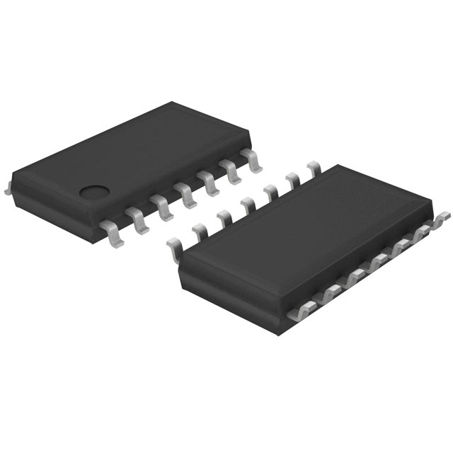
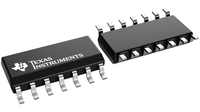
ObsoleteIC PARITY GEN/CHKER 9-BIT 14DIP
SN74AS286N
ObsoleteIC PARITY GEN/CHKER 9-BIT 14DIP
Description
General part information
74AS286 Series
The SN54AS286 and SN74AS286 universal 9-bit parity generators/checkers feature a local output for parity checking and a 48-mA bus-drivingparity input/output (I/O) port for parity generation/checking. The word-length capability is easily expanded by cascading.
The transmit () control input is implemented specifically to accommodate cascading. Whenis low, the parity tree is disabled and PARITY ERROR remains at a high logic level regardless of the input levels. Whenis high, the parity tree is enabled. PARITY ERROR indicates a parity error when either an even number of inputs (A-I) are high and PARITY I/O is forced to a low logic level, or when an odd number of inputs are high and PARITY I/O is forced to a high logic level.
The I/O control circuitry was designed so that the I/O port remains in the high-impedance state during power up or power down to prevent bus glitches.
Technical Specifications
Parameters and characteristics for this part
| Specification | SN74AS286N |
|---|---|
| Current - Output High (Max) | 48 mA |
| Current - Output High (Min) | 15 mA |
| Current - Output Low (Max) | 20 mA |
| Current - Output Low (Min) | 2 mA |
| Logic Type | Generator/Checker, Parity |
| Mounting Type | Through Hole |
| Number of Circuits (Bit) | 9 Bit |
| Operating Temperature (Max) | 70 °C |
| Operating Temperature (Min) | 0 °C |
| Package Length | 0.3 in |
| Package Name | 14-DIP, 14-PDIP |
| Package Width | 7.62 mm |
| Voltage - Supply (Maximum) | 5.5 V |
| Voltage - Supply (Minimum) | 4.5 V |
Pricing
Prices provided here are for design reference only. For realtime values and availability, please visit the distributors directly
Sign in to see pricing
Create a free account to access distributor pricing data.
CAD
3D models and CAD resources for this part
Documents
Technical documentation and resources
No documents available