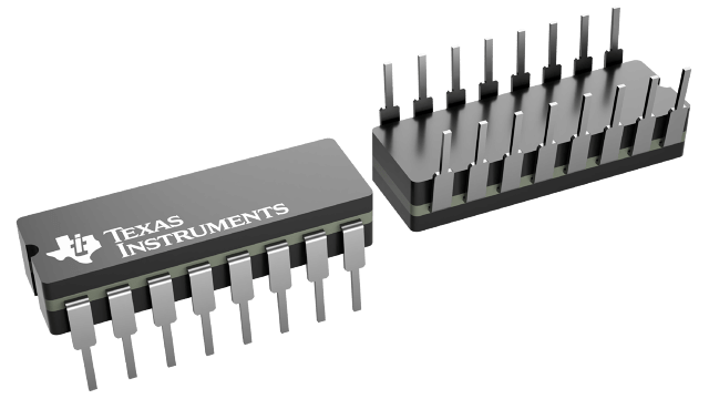
CD54HC4316F3A
ActiveHIGH SPEED CMOS LOGIC QUAD ANALOG SWITCH WITH LEVEL TRANSLATION
Deep-Dive with AI
Search across all available documentation for this part.

CD54HC4316F3A
ActiveHIGH SPEED CMOS LOGIC QUAD ANALOG SWITCH WITH LEVEL TRANSLATION
Deep-Dive with AI
Technical Specifications
Parameters and characteristics for this part
| Specification | CD54HC4316F3A |
|---|---|
| -3db Bandwidth | 200 MHz |
| Channel Capacitance (CS(off), CD(off)) [custom] | 5 pF |
| Channel Capacitance (CS(off), CD(off)) [custom] | 5 pF |
| Channel-to-Channel Matching (ΔRon) | 5 Ohm |
| Current - Leakage (IS(off)) (Max) [Max] | 100 nA |
| Mounting Type | Through Hole |
| Multiplexer/Demultiplexer Circuit | 1:1 |
| Number of Circuits | 4 |
| On-State Resistance (Max) [Max] | 170 Ohm |
| Operating Temperature [Max] | 125 °C |
| Operating Temperature [Min] | -55 C |
| Package / Case | 16-CDIP (0.300", 7.62mm) |
| Supplier Device Package | 16-CDIP |
| Switch Circuit | SPST - NO |
| Switch Time (Ton, Toff) (Max) [custom] | 37 ns |
| Switch Time (Ton, Toff) (Max) [custom] | 37 ns |
| Voltage - Supply, Single (V+) [Max] | 6 V |
| Voltage - Supply, Single (V+) [Min] | 2 V |
Pricing
Prices provided here are for design reference only. For realtime values and availability, please visit the distributors directly
CD54HC4316 Series
High Speed CMOS Logic Quad Analog Switch with Level Translation
| Part | Switch Circuit | Multiplexer/Demultiplexer Circuit | Current - Leakage (IS(off)) (Max) [Max] | Channel Capacitance (CS(off), CD(off)) [custom] | Channel Capacitance (CS(off), CD(off)) [custom] | Number of Circuits | Package / Case | Switch Time (Ton, Toff) (Max) [custom] | Switch Time (Ton, Toff) (Max) [custom] | Mounting Type | -3db Bandwidth | Operating Temperature [Min] | Operating Temperature [Max] | On-State Resistance (Max) [Max] | Voltage - Supply, Single (V+) [Min] | Voltage - Supply, Single (V+) [Max] | Supplier Device Package | Channel-to-Channel Matching (ΔRon) |
|---|---|---|---|---|---|---|---|---|---|---|---|---|---|---|---|---|---|---|
Texas Instruments CD54HC4316F3AThe ’HC4316 and CD74HCT4316 contain four independent digitally controlled analog switches that use silicon-gate CMOS technology to achieve operating speeds similar to LSTTL with the low power consumption of standard CMOS integrated circuits.
In addition these devices contain logic-level translation circuits that provide for analog signal switching of voltages between ±5V via 5V logic. Each switch is turned on by a high-level voltage on its select input (S) when the common Enable (E) is Low. A High E disables all switches. The digital inputs can swing between VCC and GND; the analog inputs/outputs can swing between VCC as a positive limit and VEE as a negative limit. Voltage ranges are shown in Figure 13-1 and Figure 13-2.
The ’HC4316 and CD74HCT4316 contain four independent digitally controlled analog switches that use silicon-gate CMOS technology to achieve operating speeds similar to LSTTL with the low power consumption of standard CMOS integrated circuits.
In addition these devices contain logic-level translation circuits that provide for analog signal switching of voltages between ±5V via 5V logic. Each switch is turned on by a high-level voltage on its select input (S) when the common Enable (E) is Low. A High E disables all switches. The digital inputs can swing between VCC and GND; the analog inputs/outputs can swing between VCC as a positive limit and VEE as a negative limit. Voltage ranges are shown in Figure 13-1 and Figure 13-2. | SPST - NO | 1:1 | 100 nA | 5 pF | 5 pF | 4 | 16-CDIP (0.300", 7.62mm) | 37 ns | 37 ns | Through Hole | 200 MHz | -55 C | 125 °C | 170 Ohm | 2 V | 6 V | 16-CDIP | 5 Ohm |
Description
General part information
CD54HC4316 Series
The ’HC4316 and CD74HCT4316 contain four independent digitally controlled analog switches that use silicon-gate CMOS technology to achieve operating speeds similar to LSTTL with the low power consumption of standard CMOS integrated circuits.
In addition these devices contain logic-level translation circuits that provide for analog signal switching of voltages between ±5V via 5V logic. Each switch is turned on by a high-level voltage on its select input (S) when the common Enable (E) is Low. A High E disables all switches. The digital inputs can swing between VCC and GND; the analog inputs/outputs can swing between VCC as a positive limit and VEE as a negative limit. Voltage ranges are shown in Figure 13-1 and Figure 13-2.
The ’HC4316 and CD74HCT4316 contain four independent digitally controlled analog switches that use silicon-gate CMOS technology to achieve operating speeds similar to LSTTL with the low power consumption of standard CMOS integrated circuits.
Documents
Technical documentation and resources


