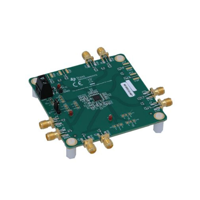
LMK1D1208EVM
ActiveCLOCK & TIMER DEVELOPMENT TOOLS
LMK1D1208EVM
ActiveCLOCK & TIMER DEVELOPMENT TOOLS
Description
General part information
LMK1D1208 Series
The LMK1D120x clock buffer distributes one of two selectable clock inputs (IN0 and IN1) to 4 or 8 pairs of differential LVDS clock outputs (OUT0 through OUT7) with minimum skew for clock distribution. The LMK1D12x family can accept two clock sources into an input multiplexer. The inputs can either be LVDS, LVPECL, LP-HCSL, HCSL, CML or LVCMOS.
The LMK1D12x is specifically designed for driving 50-Ω transmission lines. In case of driving the inputs in single-ended mode, the appropriate bias voltage as shown in must be applied to the unused negative input pin.
The IN_SEL pin selects the input which is routed to the outputs. If this pin is left open, it disables the outputs (logic low). The part supports a fail-safe function. The device further incorporates an input hysteresis which prevents random oscillation of the outputs in the absence of an input signal.
Technical Specifications
Parameters and characteristics for this part
| Specification | LMK1D1208EVM |
|---|---|
| Contents | Board |
| Embedded | No |
| Function | Clock Buffer |
| Primary Attributes | 8-Channel (Octal) |
| Secondary Attributes | On-Board Test Points |
| Supplied Contents | Board(s) |
| Type | Timing |
| Utilized IC / Part | LMK1D1208 |
Pricing
Prices provided here are for design reference only. For realtime values and availability, please visit the distributors directly
Sign in to see pricing
Create a free account to access distributor pricing data.
CAD
3D models and CAD resources for this part
Documents
Technical documentation and resources