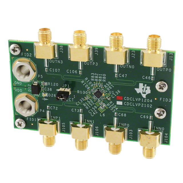
CDCLVP1204EVM
ActiveEVAL MODULE FOR CDCLVP1204
CDCLVP1204EVM
ActiveEVAL MODULE FOR CDCLVP1204
Description
General part information
CDCLVP1204 Series
The CDCLVP1204 is a highly versatile, low additive jitter buffer that can generate four copies of LVPECL clock outputs from one of two selectable LVPECL, LVDS, or LVCMOS inputs for a variety of communication applications. It has a maximum clock frequency up to 2 GHz. The CDCLVP1204 features an on-chip multiplexer (MUX) for selecting one of two inputs that can be easily configured solely through a control terminal. The overall additive jitter performance is less than 0.1 ps, RMS from 10 kHz to 20 MHz, and overall output skew is as low as 15 ps, making the device a perfect choice for use in demanding applications.
The CDCLVP1204 clock buffer distributes one of two selectable clock inputs (IN0, IN1) to four pairs of differential LVPECL clock outputs (OUT0, OUT3) with minimum skew for clock distribution. The CDCLVP1204 can accept two clock sources into an input multiplexer. The inputs can be LVPECL, LVDS, or LVCMOS/LVTTL.
The CDCLVP1204 is specifically designed for driving 50-Ω transmission lines. When driving the inputs in single-ended mode, the LVPECL bias voltage (VAC_REF) must be applied to the unused negative input terminal. However, for high-speed performance up to 2 GHz, differential mode is strongly recommended.
Technical Specifications
Parameters and characteristics for this part
| Specification | CDCLVP1204EVM |
|---|---|
| Contents | Board |
| Embedded | No |
| Function | Clock Buffer |
| Supplied Contents | Board(s) |
| Type | Timing |
| Utilized IC / Part | CDCLVP1204 |
Pricing
Prices provided here are for design reference only. For realtime values and availability, please visit the distributors directly
Sign in to see pricing
Create a free account to access distributor pricing data.
CAD
3D models and CAD resources for this part
Documents
Technical documentation and resources