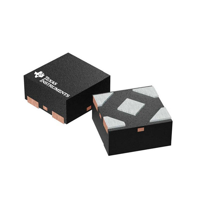
CDCBT1001DPWR
Active1.2-V TO 1.8-V CLOCK BUFFER AND LEVEL TRANSLATOR 5-X2SON -40 TO 85
Deep-Dive with AI
Search across all available documentation for this part.

CDCBT1001DPWR
Active1.2-V TO 1.8-V CLOCK BUFFER AND LEVEL TRANSLATOR 5-X2SON -40 TO 85
Deep-Dive with AI
Technical Specifications
Parameters and characteristics for this part
| Specification | CDCBT1001DPWR |
|---|---|
| Differential - Input:Output [custom] | False |
| Differential - Input:Output [custom] | False |
| Frequency - Max [Max] | 24 MHz |
| Input | LVCMOS |
| Mounting Type | Surface Mount |
| Number of Circuits | 1 |
| Operating Temperature [Max] | 85 °C |
| Operating Temperature [Min] | -40 °C |
| Output | LVCMOS |
| Package / Case | 4-XFDFN Exposed Pad |
| Ratio - Input:Output [custom] | 1:1 |
| Supplier Device Package | 5-X2SON (0.8x0.8) |
| Type | Clock Buffer |
| Voltage - Supply [Max] | 1.32 V |
| Voltage - Supply [Min] | 1.08 V |
Pricing
Prices provided here are for design reference only. For realtime values and availability, please visit the distributors directly
| Distributor | Package | Quantity | $ | |
|---|---|---|---|---|
| DigiKey | Digi-Reel®, Cut Tape (CT), Tape & Reel (TR) | 1 | $ 1.42 | |
| 10 | $ 1.04 | |||
| 25 | $ 0.94 | |||
| 100 | $ 0.83 | |||
| 250 | $ 0.78 | |||
| 500 | $ 0.75 | |||
| 1000 | $ 0.73 | |||
| 3000 | $ 0.70 | |||
| 6000 | $ 0.68 | |||
| 9000 | $ 0.67 | |||
| 15000 | $ 0.66 | |||
| Digikey | Cut Tape (CT) | 1 | $ 1.49 | |
| 10 | $ 1.34 | |||
| 25 | $ 1.26 | |||
| 100 | $ 1.08 | |||
| 250 | $ 1.01 | |||
| 500 | $ 0.88 | |||
| 1000 | $ 0.73 | |||
| Digi-Reel® | 1 | $ 1.49 | ||
| 10 | $ 1.34 | |||
| 25 | $ 1.26 | |||
| 100 | $ 1.08 | |||
| 250 | $ 1.01 | |||
| 500 | $ 0.88 | |||
| 1000 | $ 0.73 | |||
| Tape & Reel (TR) | 3000 | $ 0.63 | ||
| Mouser Electronics | N/A | 1 | $ 1.42 | |
| 10 | $ 0.94 | |||
| 100 | $ 0.83 | |||
| 250 | $ 0.78 | |||
| 500 | $ 0.75 | |||
| 1000 | $ 0.73 | |||
| 3000 | $ 0.68 | |||
| 6000 | $ 0.67 | |||
| 9000 | $ 0.66 | |||
| Texas Instruments | LARGE T&R | 1 | $ 1.12 | |
| 100 | $ 0.93 | |||
| 250 | $ 0.67 | |||
| 1000 | $ 0.50 | |||
CDCBT1001 Series
1.2-V to 1.8-V clock buffer and level translator
| Part | Supplier Device Package | Frequency - Max [Max] | Mounting Type | Output | Type | Differential - Input:Output [custom] | Differential - Input:Output [custom] | Number of Circuits | Package / Case | Input | Voltage - Supply [Min] | Voltage - Supply [Max] | Operating Temperature [Max] | Operating Temperature [Min] | Ratio - Input:Output [custom] |
|---|---|---|---|---|---|---|---|---|---|---|---|---|---|---|---|
Texas Instruments CDCBT1001DPWR | 5-X2SON (0.8x0.8) | 24 MHz | Surface Mount | LVCMOS | Clock Buffer | 1 | 4-XFDFN Exposed Pad | LVCMOS | 1.08 V | 1.32 V | 85 °C | -40 °C | 1:1 |
Description
General part information
CDCBT1001 Series
The CDCBT1001 is a 1.2-V to 1.8-V clock buffer and level translator. The VDD_IN pin supply voltage defines the input LVCMOS clock level. The VDD_OUT pin supply voltage defines the output LVCMOS clock level. VDD_IN = 1.2 V ± 10%. VDD_OUT = 1.8 V ± 10%
The 12-kHz to 5-MHz additive RMS jitter at 24 MHz is less than 0.8 ps.
The CDCBT1001 is a 1.2-V to 1.8-V clock buffer and level translator. The VDD_IN pin supply voltage defines the input LVCMOS clock level. The VDD_OUT pin supply voltage defines the output LVCMOS clock level. VDD_IN = 1.2 V ± 10%. VDD_OUT = 1.8 V ± 10%


