


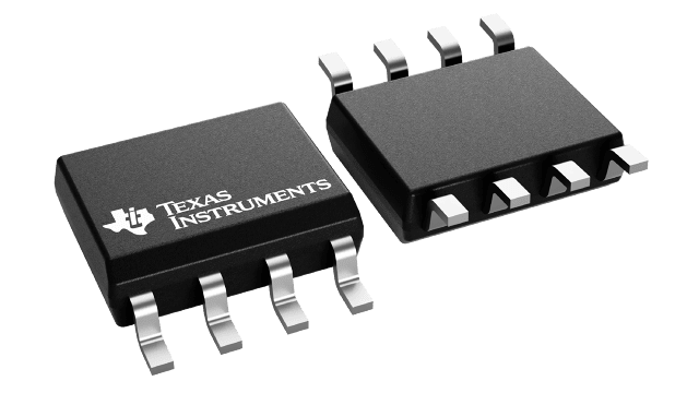
TPS2066AD
Obsolete2-CH, 1A LOADING, 1.6A ILIMIT, 2.7-5.5V, 70MΩ USB POWER SWITCH, ACTIVE-HIGH

TPS2066AD
Obsolete2-CH, 1A LOADING, 1.6A ILIMIT, 2.7-5.5V, 70MΩ USB POWER SWITCH, ACTIVE-HIGH
Description
General part information
TPS2066A Series
The TPS206xA power-distribution switches are intended for applications where heavy capacitive loads and short-circuits are likely to be encountered. The TPS206xA family is pin-for-pin compatible with the TPS206x family with a tighter overcurrent tolerance. This family of devices incorporates two 70mΩ N-channel MOSFET power switches for power-distribution systems that require multiple power switches in a single package. Each switch is controlled by a logic enable input. Gate drive is provided by an internal charge pump designed to control the power-switch rise and fall times to minimize current surges during switching. The charge pump requires no external components and allows operation from supplies as low as 2.7V.
Each device limits the output current to a safe level by switching into a constant-current mode when the output load exceeds the current-limit threshold or a short is present. Individual channels indicate the presence of an overcurrent condition by asserting its corresponding OCx output (active low). Thermal protection circuitry disables the device during overcurrent or short-circuit events to prevent permanent damage. The device recovers from thermal shutdown automatically once the device has cooled sufficiently. The device provides undervoltage lockout to disable the device until the input voltage rises above 2.0V. The TPS206xA is designed to current limit at 1.6A typically per channel.
The TPS206xA power-distribution switches are intended for applications where heavy capacitive loads and short-circuits are likely to be encountered. The TPS206xA family is pin-for-pin compatible with the TPS206x family with a tighter overcurrent tolerance. This family of devices incorporates two 70mΩ N-channel MOSFET power switches for power-distribution systems that require multiple power switches in a single package. Each switch is controlled by a logic enable input. Gate drive is provided by an internal charge pump designed to control the power-switch rise and fall times to minimize current surges during switching. The charge pump requires no external components and allows operation from supplies as low as 2.7V.
Technical Specifications
Parameters and characteristics for this part
| Specification | TPS2066AD |
|---|---|
| Current - Output (Max) | 1 A |
| Fault Protection | UVRO, Over Temperature, Current Limiting (Fixed) |
| Features | Status Flag |
| Input Ratio | 1 |
| Input Type | Non-Inverting |
| Interface | On/Off |
| Mounting Type | Surface Mount |
| Number of Outputs | 2 |
| Operating Temperature (Max) | 125 °C |
| Operating Temperature (Min) | -40 °C |
| Output Configuration | High Side |
| Output Ratio | 2 |
| Output Type | N-Channel |
| Package Length | 0.154 in |
| Package Name | 8-SOIC |
| Package Width | 3.9 mm |
| Rds On (Typ) | 70 mOhm |
| Switch Type | General Purpose |
| Voltage - Load (Max) | 5.5 V |
| Voltage - Load (Min) | 2.7 V |
| Voltage - Supply (Vcc/Vdd) | Not Required |
| Voltage - Supply (Vdd/Vcc) | Not Required |
Pricing
Prices provided here are for design reference only. For realtime values and availability, please visit the distributors directly
Sign in to see pricing
Create a free account to access distributor pricing data.
CAD
3D models and CAD resources for this part
Documents
Technical documentation and resources