CDCU877ARTBT
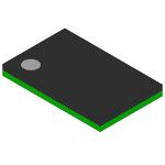
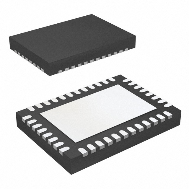
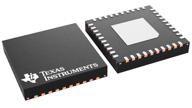
ObsoleteIC PLL CLOCK DRIVER 1.8V 40-QFN
CDCU877ARTBT
ObsoleteIC PLL CLOCK DRIVER 1.8V 40-QFN
Description
General part information
CDCU877 Series
The CDCU877 is a high-performance, low-jitter, low-skew, zero-delay buffer that distributes a differential clock input pair (CK,CK) to ten differential pairs of clock outputs (Yn,Yn) and to one differential pair of feedback clock outputs (FBOUT,FBOUT). The clock outputs are controlled by the input clocks (CK,CK), the feedback clocks (FBIN,FBIN), the LVCMOS control pins (OE, OS), and the analog power input (AVDD). When OE is low, the clock outputs, except FBOUT/FBOUT, are disabled while the internal PLL continues to maintain its locked-in frequency. OS (output select) is a program pin that must be tied to GND or VDD. When OS is high, OE functions as previously described. When OS and OE are both low, OE has no affect on Y7/Y7, they are free running. When AVDDis grounded, the PLL is turned off and bypassed for test purposes.
When both clock inputs (CK,CK) are logic low, the device enters in a low power mode. An input logic detection circuit on the differential inputs, independent from input buffers, detects the logic low level and performs in a low power state where all outputs, the feedback, and the PLL are off. When the clock inputs transition from being logic low to being differential signals, the PLL turns back on, the inputs and the outputs are enabled, and the PLL obtains phase lock between the feedback clock pair (FBIN,FBIN) and the clock input pair (CK,CK) within the specified stabilization time.
The CDCU877 is able to track spread spectrum clocking (SSC) for reduced EMI. This device operates from -40°C to 85°C.
Technical Specifications
Parameters and characteristics for this part
| Specification | CDCU877ARTBT |
|---|---|
| Differential Input | Yes |
| Differential Output | Yes |
| Frequency - Max | 400 MHz |
| Input | SSTL-18 |
| Input Ratio | 1 |
| Main Purpose | Memory, DDR2 |
| Mounting Type | Surface Mount |
| Number of Circuits | 1 |
| Operating Temperature (Max) | 85 °C |
| Operating Temperature (Min) | -40 °C |
| Output | SSTL-18 |
| Output Ratio | 10 |
| Package / Case | 40-VFQFN Exposed Pad |
| Package Length | 6 mm |
| Package Name | 40-VQFN |
| Package Width | 6 mm |
| PLL | Yes |
| Voltage - Supply (Maximum) | 1.9 V |
| Voltage - Supply (Minimum) | 1.7 V |
Pricing
Prices provided here are for design reference only. For realtime values and availability, please visit the distributors directly
Sign in to see pricing
Create a free account to access distributor pricing data.
CAD
3D models and CAD resources for this part
Documents
Technical documentation and resources