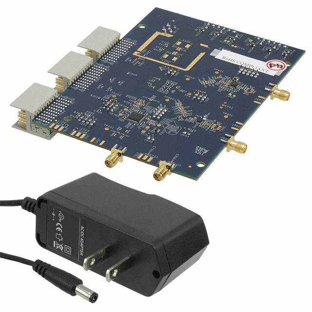
AD9628BCPZ-125
Active12-BIT, 125/105 MSPS, 1.8 V DUAL ANALOG-TO-DIGITAL CONVERTER
AD9628BCPZ-125
Active12-BIT, 125/105 MSPS, 1.8 V DUAL ANALOG-TO-DIGITAL CONVERTER
Description
General part information
AD9628 Series
The AD9628 is a monolithic, dual-channel, 1.8 V supply, 12-bit, 125 MSPS/105 MSPS analog-to-digital converter (ADC). It features a high performance sample-and-hold circuit and on-chip voltage reference.The product uses multistage differential pipeline architecture with output error correction logic to provide 12-bit accuracy at 125 MSPS data rates and to guarantee no missing codes over the full operating temperature range.The ADC contains several features designed to maximize flexibility and minimize system cost, such as programmable clock and data alignment and programmable digital test pattern generation. The available digital test patterns include built-in deterministic and pseudorandom patterns, along with custom user-defined test patterns entered via the serial port interface (SPI).A differential clock input controls all internal conversion cycles. An optional duty cycle stabilizer (DCS) compensates for wide variations in the clock duty cycle while maintaining excellent overall ADC performance.The digital output data is presented in offset binary, Gray code, or twos complement format. A data output clock (DCO) is provided for each ADC channel to ensure proper latch timing with receiving logic. 1.8 V CMOS or LVDS output logic levels are supported. Output data can also be multiplexed onto a single output bus.APPLICATIONSCommunicationsDiversity radio systemsMultimode digital receiversGSM, EDGE, W-CDMA, LTE, CDMA2000, WIMAX, TD-SCDMAI/Q demodulation systemsSmart antenna systemsBroadband data applicationsBattery-powered instrumentsHand-held scope metersPortable medical imagingUltrasoundRadar/LIDARPRODUCT HIGHLIGHTSThe AD9628 operates from a single 1.8 V analog power supply and features a separate digital output driver supply to accommodate 1.8 V CMOS or LVDS logic families.The patented sample-and-hold circuit maintains excellent performance for input frequencies up to 200 MHz and is designed for low cost, low power, and ease of use.A standard serial port interface supports various product features and functions, such as data output formatting, internal clock divider, power-down, DCO/data timing and offset adjustments.The AD9628 is packaged in a 64-lead RoHS-compliant LFCSP that is pin compatible with theAD9650/AD9269/AD926816-bit ADC, theAD9258/AD9251/AD964814-bit ADCs, the AD9231 12-bit ADC, and theAD9608/AD920410-bit ADCs, enabling a simple migration path between 10-bit and 16-bit converters sampling from 20MSPS to 125MSPS.
Technical Specifications
Parameters and characteristics for this part
| Specification | AD9628BCPZ-125 |
|---|---|
| Architecture | Pipelined |
| Configuration | S/H-ADC |
| Data Interface | LVDS - Parallel |
| Features | Simultaneous Sampling |
| Input Type | Single Ended, Differential |
| Mounting Type | Surface Mount |
| Number of A/D Converters | 2 count |
| Number of Bits | 12 bits |
| Number of Inputs | 2 |
| Operating Temperature (Max) | 85 °C |
| Operating Temperature (Min) | -40 °C |
| Package / Case | CSP, 64-VFQFN Exposed Pad |
| Package Length | 9 mm |
| Package Name | 64-LFCSP-VQ |
| Package Width | 9 mm |
| Ratio - ADC | 1 |
| Ratio - S/H | 1 |
| Reference Type | External, Internal |
| Sampling Rate (Per Second) | 125 MHz |
| Voltage - Supply, Analog (Max) | 1.9 V |
| Voltage - Supply, Analog (Min) | 1.7 V |
| Voltage - Supply, Digital (Max) | 1.9 V |
| Voltage - Supply, Digital (Min) | 1.7 V |
Pricing
Prices provided here are for design reference only. For realtime values and availability, please visit the distributors directly
Sign in to see pricing
Create a free account to access distributor pricing data.
CAD
3D models and CAD resources for this part
Documents
Technical documentation and resources