CDCDB400RHBR
Active4-OUTPUT CLOCK BUFFER FOR PCIE® GEN 1 TO GEN 6
Deep-Dive with AI
Search across all available documentation for this part.
CDCDB400RHBR
Active4-OUTPUT CLOCK BUFFER FOR PCIE® GEN 1 TO GEN 6
Deep-Dive with AI
Technical Specifications
Parameters and characteristics commom to parts in this series
| Specification | CDCDB400RHBR | CDCDB400 Series |
|---|---|---|
| Differential - Input:Output [custom] | True | True |
| Differential - Input:Output [custom] | True | True |
| Frequency - Max [Max] | 250 MHz | 250 MHz |
| Input | HCSL | HCSL |
| Mounting Type | Surface Mount | Surface Mount |
| Number of Circuits | 1 | 1 |
| Operating Temperature [Max] | 105 °C | 105 °C |
| Operating Temperature [Min] | -40 °C | -40 °C |
| Output | Clock, HCSL | Clock, HCSL |
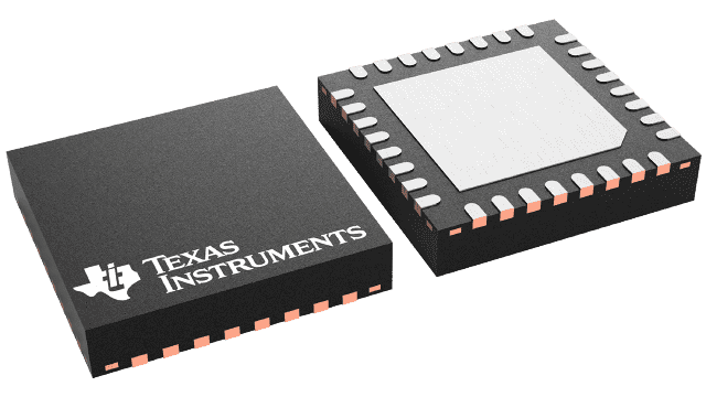
| Package / Case | 32-VFQFN Exposed Pad | 32-VFQFN Exposed Pad |
| Ratio - Input:Output [custom] | 4 | 4 |
| Ratio - Input:Output [custom] | 1 | 1 |
| Supplier Device Package | 32-VQFN (5x5) | 32-VQFN (5x5) |
| Type | Clock Buffer | Clock Buffer |
| Voltage - Supply [Max] | 3.6 V | 3.6 V |
| Voltage - Supply [Min] | 3 V | 3 V |
Pricing
Prices provided here are for design reference only. For realtime values and availability, please visit the distributors directly
| Distributor | Package | Quantity | $ | |
|---|---|---|---|---|
| Digikey | Cut Tape (CT) | 1 | $ 3.65 | |
| 10 | $ 3.28 | |||
| 25 | $ 3.10 | |||
| 100 | $ 2.69 | |||
| 250 | $ 2.55 | |||
| 500 | $ 2.29 | |||
| 1000 | $ 1.93 | |||
| Digi-Reel® | 1 | $ 3.65 | ||
| 10 | $ 3.28 | |||
| 25 | $ 3.10 | |||
| 100 | $ 2.69 | |||
| 250 | $ 2.55 | |||
| 500 | $ 2.29 | |||
| 1000 | $ 1.93 | |||
| Tape & Reel (TR) | 3000 | $ 1.38 | ||
| Texas Instruments | LARGE T&R | 1 | $ 2.22 | |
| 100 | $ 1.95 | |||
| 250 | $ 1.36 | |||
| 1000 | $ 1.10 | |||
CDCDB400 Series
4-output clock buffer for PCIe® Gen 1 to Gen 6
| Part | Differential - Input:Output [custom] | Differential - Input:Output [custom] | Voltage - Supply [Max] | Voltage - Supply [Min] | Mounting Type | Operating Temperature [Max] | Operating Temperature [Min] | Supplier Device Package | Input | Ratio - Input:Output [custom] | Ratio - Input:Output [custom] | Package / Case | Frequency - Max [Max] | Type | Number of Circuits | Output |
|---|---|---|---|---|---|---|---|---|---|---|---|---|---|---|---|---|
Texas Instruments CDCDB400RHBR | 3.6 V | 3 V | Surface Mount | 105 °C | -40 °C | 32-VQFN (5x5) | HCSL | 4 | 1 | 32-VFQFN Exposed Pad | 250 MHz | Clock Buffer | 1 | Clock, HCSL | ||
Texas Instruments CDCDB400RHBT | 3.6 V | 3 V | Surface Mount | 105 °C | -40 °C | 32-VQFN (5x5) | HCSL | 4 | 1 | 32-VFQFN Exposed Pad | 250 MHz | Clock Buffer | 1 | Clock, HCSL |
Description
General part information
CDCDB400 Series
The CDCDB400 is a 4-output LP-HCSL, DB800ZL-compliant, clock buffer capable of distributing the reference clock for PCIe Gen 1-6, QuickPath Interconnect (QPI), UPI, SAS, and SATA interfaces in CC, SRNS, or SRIS architectures. The SMBus interface and four output enable pins allow the configuration and control of all four outputs individually. The CDCDB400 is a DB800ZL derivative buffer and meets or exceeds the system parameters in the DB800ZL specification. The device also meets or exceeds the parameters in the DB2000Q specification. The CDCDB400 is packaged in a 5-mm × 5-mm, 32-pin VQFN package.
The CDCDB400 is a 4-output LP-HCSL, DB800ZL-compliant, clock buffer capable of distributing the reference clock for PCIe Gen 1-6, QuickPath Interconnect (QPI), UPI, SAS, and SATA interfaces in CC, SRNS, or SRIS architectures. The SMBus interface and four output enable pins allow the configuration and control of all four outputs individually. The CDCDB400 is a DB800ZL derivative buffer and meets or exceeds the system parameters in the DB800ZL specification. The device also meets or exceeds the parameters in the DB2000Q specification. The CDCDB400 is packaged in a 5-mm × 5-mm, 32-pin VQFN package.
Documents
Technical documentation and resources