TPS75925KC
Active7.5-A, ULTRA-LOW-DROPOUT VOLTAGE REGULATOR WITH POWER GOOD & ENABLE
Deep-Dive with AI
Search across all available documentation for this part.
TPS75925KC
Active7.5-A, ULTRA-LOW-DROPOUT VOLTAGE REGULATOR WITH POWER GOOD & ENABLE
Technical Specifications
Parameters and characteristics commom to parts in this series
| Specification | TPS75925KC | TPS759 Series |
|---|---|---|
| Control Features | Power Good, Enable | Power Good, Enable |
| Current - Output | 7.5 A | 7.5 A |
| Current - Quiescent (Iq) | 200 µA | 200 µA |
| Mounting Type | Through Hole | Surface Mount, Through Hole |
| Number of Regulators | 1 | 1 |
| Operating Temperature [Max] | 125 °C | 125 °C |
| Operating Temperature [Min] | -40 °C | -40 °C |
| Output Configuration | Positive | Positive |
| Output Type | 27.03 °C/W | 27.03 °C/W |
| Output Type | - | Adjustable |
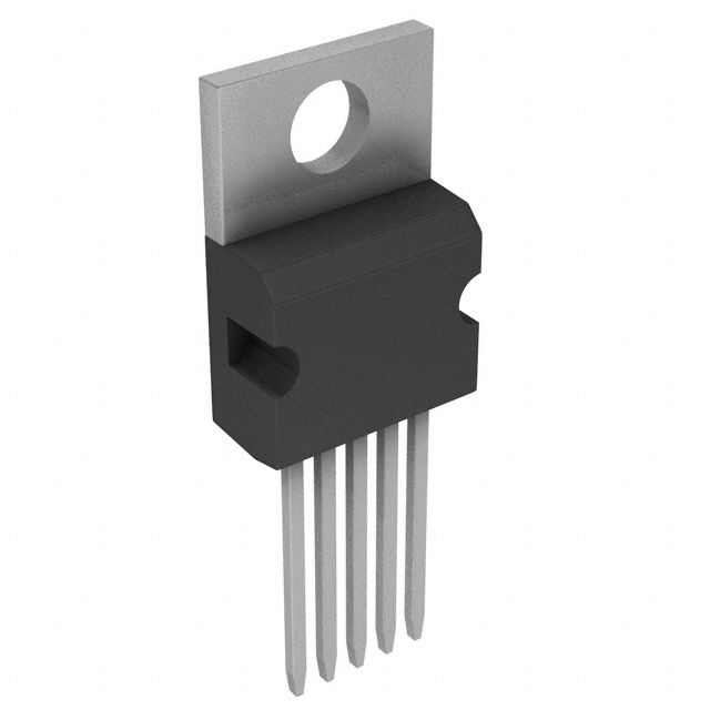
| Package / Case | TO-220-5 | TO-263BA, D2PAK (5 Leads + Tab), TO-263-6, TO-220-5 |
| Protection Features | Over Current, Reverse Polarity, Under Voltage Lockout (UVLO), Over Temperature | Over Current, Reverse Polarity, Under Voltage Lockout (UVLO), Over Temperature |
| PSRR | 58 dB | 58 dB |
| Supplier Device Package | TO-220-5 | TO-263 (DDPAK-5), TO-220-5 |
| Voltage - Input (Max) [Max] | 5.5 V | 5.5 V |
| Voltage - Output (Max) | - | 5 V |
| Voltage - Output (Min/Fixed) | 2.5 V | 1.5 - 3.3 V |
| Voltage Dropout (Max) | - | 0.75 V |
Pricing
Prices provided here are for design reference only. For realtime values and availability, please visit the distributors directly
TPS759 Series
7.5-A, ultra-low-dropout voltage regulator with power good & enable
| Part | Voltage - Output (Min/Fixed) | Number of Regulators | PSRR | Mounting Type | Control Features | Voltage - Input (Max) [Max] | Output Type | Current - Output | Protection Features | Package / Case | Current - Quiescent (Iq) | Output Configuration | Supplier Device Package | Operating Temperature [Max] | Operating Temperature [Min] | Voltage Dropout (Max) [Max] | Voltage - Output (Max) [Max] | Output Type |
|---|---|---|---|---|---|---|---|---|---|---|---|---|---|---|---|---|---|---|
Texas Instruments TPS75915KTTRThe TPS759xx family of 7.5-A low dropout (LDO) regulators contains four fixed voltage option regulators with integrated power-good (PG)\ and an adjustable voltage option regulator. These devices are capable of supplying 7.5 A of output current with a dropout of 400 mV (TPS75933). Therefore, the devices are capable of performing a 3.3-V to 2.5-V conversion. Quiescent current is 125 uA at full load and drops below 10 µA when the devices are disabled. The TPS759xx is designed to have fast transient response for large load current changes.
Because the PMOS device behaves as a low-value resistor, the dropout voltage is very low (typically 400 mV at an output current of 7.5 A for the TPS75933) and is directly proportional to the output current. Additionally, since the PMOS pass element is a voltage-driven device, the quiescent current is very low and independent of output loading (typically 125 µA over the full range of output current, 1 mA to 7.5 A). These two key specifications yield a significant improvement in operating life for battery-powered systems.
The device is enabled when EN\ is connected to a low-level voltage. This LDO family also features a sleep mode; applying a TTL high signal to EN\ (enable) shuts down the regulator, reducing the quiescent current to less than 1 µA at TJ= 25°C. The power-good terminal (PG)\ is an active low, open drain output, which can be used to implement a power-on reset or a low-battery indicator.
The TPS759xx is offered in 1.5-V, 1.8-V, 2.5-V, and 3.3-V fixed-voltage versions and in an adjustable version (programmable over the range of 1.22 V to 5 V). Output voltage tolerance is specified as a maximum of 3% over line, load, and temperature ranges. The TPS759xx family is available in a 5-pin TO–220 (KC) and TO–263 (KTT) packages.
The TPS759xx family of 7.5-A low dropout (LDO) regulators contains four fixed voltage option regulators with integrated power-good (PG)\ and an adjustable voltage option regulator. These devices are capable of supplying 7.5 A of output current with a dropout of 400 mV (TPS75933). Therefore, the devices are capable of performing a 3.3-V to 2.5-V conversion. Quiescent current is 125 uA at full load and drops below 10 µA when the devices are disabled. The TPS759xx is designed to have fast transient response for large load current changes.
Because the PMOS device behaves as a low-value resistor, the dropout voltage is very low (typically 400 mV at an output current of 7.5 A for the TPS75933) and is directly proportional to the output current. Additionally, since the PMOS pass element is a voltage-driven device, the quiescent current is very low and independent of output loading (typically 125 µA over the full range of output current, 1 mA to 7.5 A). These two key specifications yield a significant improvement in operating life for battery-powered systems.
The device is enabled when EN\ is connected to a low-level voltage. This LDO family also features a sleep mode; applying a TTL high signal to EN\ (enable) shuts down the regulator, reducing the quiescent current to less than 1 µA at TJ= 25°C. The power-good terminal (PG)\ is an active low, open drain output, which can be used to implement a power-on reset or a low-battery indicator.
The TPS759xx is offered in 1.5-V, 1.8-V, 2.5-V, and 3.3-V fixed-voltage versions and in an adjustable version (programmable over the range of 1.22 V to 5 V). Output voltage tolerance is specified as a maximum of 3% over line, load, and temperature ranges. The TPS759xx family is available in a 5-pin TO–220 (KC) and TO–263 (KTT) packages. | 1.5 V | 1 | 58 dB | Surface Mount | Enable, Power Good | 5.5 V | 27.03 °C/W | 7.5 A | Over Current, Over Temperature, Reverse Polarity, Under Voltage Lockout (UVLO) | D2PAK (5 Leads + Tab), TO-263-6, TO-263BA | 200 µA | Positive | TO-263 (DDPAK-5) | 125 °C | -40 °C | |||
Texas Instruments TPS75925KCThe TPS759xx family of 7.5-A low dropout (LDO) regulators contains four fixed voltage option regulators with integrated power-good (PG)\ and an adjustable voltage option regulator. These devices are capable of supplying 7.5 A of output current with a dropout of 400 mV (TPS75933). Therefore, the devices are capable of performing a 3.3-V to 2.5-V conversion. Quiescent current is 125 uA at full load and drops below 10 µA when the devices are disabled. The TPS759xx is designed to have fast transient response for large load current changes.
Because the PMOS device behaves as a low-value resistor, the dropout voltage is very low (typically 400 mV at an output current of 7.5 A for the TPS75933) and is directly proportional to the output current. Additionally, since the PMOS pass element is a voltage-driven device, the quiescent current is very low and independent of output loading (typically 125 µA over the full range of output current, 1 mA to 7.5 A). These two key specifications yield a significant improvement in operating life for battery-powered systems.
The device is enabled when EN\ is connected to a low-level voltage. This LDO family also features a sleep mode; applying a TTL high signal to EN\ (enable) shuts down the regulator, reducing the quiescent current to less than 1 µA at TJ= 25°C. The power-good terminal (PG)\ is an active low, open drain output, which can be used to implement a power-on reset or a low-battery indicator.
The TPS759xx is offered in 1.5-V, 1.8-V, 2.5-V, and 3.3-V fixed-voltage versions and in an adjustable version (programmable over the range of 1.22 V to 5 V). Output voltage tolerance is specified as a maximum of 3% over line, load, and temperature ranges. The TPS759xx family is available in a 5-pin TO–220 (KC) and TO–263 (KTT) packages.
The TPS759xx family of 7.5-A low dropout (LDO) regulators contains four fixed voltage option regulators with integrated power-good (PG)\ and an adjustable voltage option regulator. These devices are capable of supplying 7.5 A of output current with a dropout of 400 mV (TPS75933). Therefore, the devices are capable of performing a 3.3-V to 2.5-V conversion. Quiescent current is 125 uA at full load and drops below 10 µA when the devices are disabled. The TPS759xx is designed to have fast transient response for large load current changes.
Because the PMOS device behaves as a low-value resistor, the dropout voltage is very low (typically 400 mV at an output current of 7.5 A for the TPS75933) and is directly proportional to the output current. Additionally, since the PMOS pass element is a voltage-driven device, the quiescent current is very low and independent of output loading (typically 125 µA over the full range of output current, 1 mA to 7.5 A). These two key specifications yield a significant improvement in operating life for battery-powered systems.
The device is enabled when EN\ is connected to a low-level voltage. This LDO family also features a sleep mode; applying a TTL high signal to EN\ (enable) shuts down the regulator, reducing the quiescent current to less than 1 µA at TJ= 25°C. The power-good terminal (PG)\ is an active low, open drain output, which can be used to implement a power-on reset or a low-battery indicator.
The TPS759xx is offered in 1.5-V, 1.8-V, 2.5-V, and 3.3-V fixed-voltage versions and in an adjustable version (programmable over the range of 1.22 V to 5 V). Output voltage tolerance is specified as a maximum of 3% over line, load, and temperature ranges. The TPS759xx family is available in a 5-pin TO–220 (KC) and TO–263 (KTT) packages. | 2.5 V | 1 | 58 dB | Through Hole | Enable, Power Good | 5.5 V | 27.03 °C/W | 7.5 A | Over Current, Over Temperature, Reverse Polarity, Under Voltage Lockout (UVLO) | TO-220-5 | 200 µA | Positive | TO-220-5 | 125 °C | -40 °C | |||
Texas Instruments TPS75933KTTRThe TPS759xx family of 7.5-A low dropout (LDO) regulators contains four fixed voltage option regulators with integrated power-good (PG)\ and an adjustable voltage option regulator. These devices are capable of supplying 7.5 A of output current with a dropout of 400 mV (TPS75933). Therefore, the devices are capable of performing a 3.3-V to 2.5-V conversion. Quiescent current is 125 uA at full load and drops below 10 µA when the devices are disabled. The TPS759xx is designed to have fast transient response for large load current changes.
Because the PMOS device behaves as a low-value resistor, the dropout voltage is very low (typically 400 mV at an output current of 7.5 A for the TPS75933) and is directly proportional to the output current. Additionally, since the PMOS pass element is a voltage-driven device, the quiescent current is very low and independent of output loading (typically 125 µA over the full range of output current, 1 mA to 7.5 A). These two key specifications yield a significant improvement in operating life for battery-powered systems.
The device is enabled when EN\ is connected to a low-level voltage. This LDO family also features a sleep mode; applying a TTL high signal to EN\ (enable) shuts down the regulator, reducing the quiescent current to less than 1 µA at TJ= 25°C. The power-good terminal (PG)\ is an active low, open drain output, which can be used to implement a power-on reset or a low-battery indicator.
The TPS759xx is offered in 1.5-V, 1.8-V, 2.5-V, and 3.3-V fixed-voltage versions and in an adjustable version (programmable over the range of 1.22 V to 5 V). Output voltage tolerance is specified as a maximum of 3% over line, load, and temperature ranges. The TPS759xx family is available in a 5-pin TO–220 (KC) and TO–263 (KTT) packages.
The TPS759xx family of 7.5-A low dropout (LDO) regulators contains four fixed voltage option regulators with integrated power-good (PG)\ and an adjustable voltage option regulator. These devices are capable of supplying 7.5 A of output current with a dropout of 400 mV (TPS75933). Therefore, the devices are capable of performing a 3.3-V to 2.5-V conversion. Quiescent current is 125 uA at full load and drops below 10 µA when the devices are disabled. The TPS759xx is designed to have fast transient response for large load current changes.
Because the PMOS device behaves as a low-value resistor, the dropout voltage is very low (typically 400 mV at an output current of 7.5 A for the TPS75933) and is directly proportional to the output current. Additionally, since the PMOS pass element is a voltage-driven device, the quiescent current is very low and independent of output loading (typically 125 µA over the full range of output current, 1 mA to 7.5 A). These two key specifications yield a significant improvement in operating life for battery-powered systems.
The device is enabled when EN\ is connected to a low-level voltage. This LDO family also features a sleep mode; applying a TTL high signal to EN\ (enable) shuts down the regulator, reducing the quiescent current to less than 1 µA at TJ= 25°C. The power-good terminal (PG)\ is an active low, open drain output, which can be used to implement a power-on reset or a low-battery indicator.
The TPS759xx is offered in 1.5-V, 1.8-V, 2.5-V, and 3.3-V fixed-voltage versions and in an adjustable version (programmable over the range of 1.22 V to 5 V). Output voltage tolerance is specified as a maximum of 3% over line, load, and temperature ranges. The TPS759xx family is available in a 5-pin TO–220 (KC) and TO–263 (KTT) packages. | 3.3 V | 1 | 58 dB | Surface Mount | Enable, Power Good | 5.5 V | 27.03 °C/W | 7.5 A | Over Current, Over Temperature, Reverse Polarity, Under Voltage Lockout (UVLO) | D2PAK (5 Leads + Tab), TO-263-6, TO-263BA | 200 µA | Positive | TO-263 (DDPAK-5) | 125 °C | -40 °C | 0.75 V | ||
Texas Instruments TPS75918KTTTThe TPS759xx family of 7.5-A low dropout (LDO) regulators contains four fixed voltage option regulators with integrated power-good (PG)\ and an adjustable voltage option regulator. These devices are capable of supplying 7.5 A of output current with a dropout of 400 mV (TPS75933). Therefore, the devices are capable of performing a 3.3-V to 2.5-V conversion. Quiescent current is 125 uA at full load and drops below 10 µA when the devices are disabled. The TPS759xx is designed to have fast transient response for large load current changes.
Because the PMOS device behaves as a low-value resistor, the dropout voltage is very low (typically 400 mV at an output current of 7.5 A for the TPS75933) and is directly proportional to the output current. Additionally, since the PMOS pass element is a voltage-driven device, the quiescent current is very low and independent of output loading (typically 125 µA over the full range of output current, 1 mA to 7.5 A). These two key specifications yield a significant improvement in operating life for battery-powered systems.
The device is enabled when EN\ is connected to a low-level voltage. This LDO family also features a sleep mode; applying a TTL high signal to EN\ (enable) shuts down the regulator, reducing the quiescent current to less than 1 µA at TJ= 25°C. The power-good terminal (PG)\ is an active low, open drain output, which can be used to implement a power-on reset or a low-battery indicator.
The TPS759xx is offered in 1.5-V, 1.8-V, 2.5-V, and 3.3-V fixed-voltage versions and in an adjustable version (programmable over the range of 1.22 V to 5 V). Output voltage tolerance is specified as a maximum of 3% over line, load, and temperature ranges. The TPS759xx family is available in a 5-pin TO–220 (KC) and TO–263 (KTT) packages.
The TPS759xx family of 7.5-A low dropout (LDO) regulators contains four fixed voltage option regulators with integrated power-good (PG)\ and an adjustable voltage option regulator. These devices are capable of supplying 7.5 A of output current with a dropout of 400 mV (TPS75933). Therefore, the devices are capable of performing a 3.3-V to 2.5-V conversion. Quiescent current is 125 uA at full load and drops below 10 µA when the devices are disabled. The TPS759xx is designed to have fast transient response for large load current changes.
Because the PMOS device behaves as a low-value resistor, the dropout voltage is very low (typically 400 mV at an output current of 7.5 A for the TPS75933) and is directly proportional to the output current. Additionally, since the PMOS pass element is a voltage-driven device, the quiescent current is very low and independent of output loading (typically 125 µA over the full range of output current, 1 mA to 7.5 A). These two key specifications yield a significant improvement in operating life for battery-powered systems.
The device is enabled when EN\ is connected to a low-level voltage. This LDO family also features a sleep mode; applying a TTL high signal to EN\ (enable) shuts down the regulator, reducing the quiescent current to less than 1 µA at TJ= 25°C. The power-good terminal (PG)\ is an active low, open drain output, which can be used to implement a power-on reset or a low-battery indicator.
The TPS759xx is offered in 1.5-V, 1.8-V, 2.5-V, and 3.3-V fixed-voltage versions and in an adjustable version (programmable over the range of 1.22 V to 5 V). Output voltage tolerance is specified as a maximum of 3% over line, load, and temperature ranges. The TPS759xx family is available in a 5-pin TO–220 (KC) and TO–263 (KTT) packages. | 1.8 V | 1 | 58 dB | Surface Mount | Enable, Power Good | 5.5 V | 27.03 °C/W | 7.5 A | Over Current, Over Temperature, Reverse Polarity, Under Voltage Lockout (UVLO) | D2PAK (5 Leads + Tab), TO-263-6, TO-263BA | 200 µA | Positive | TO-263 (DDPAK-5) | 125 °C | -40 °C | |||
Texas Instruments TPS75915KCThe TPS759xx family of 7.5-A low dropout (LDO) regulators contains four fixed voltage option regulators with integrated power-good (PG)\ and an adjustable voltage option regulator. These devices are capable of supplying 7.5 A of output current with a dropout of 400 mV (TPS75933). Therefore, the devices are capable of performing a 3.3-V to 2.5-V conversion. Quiescent current is 125 uA at full load and drops below 10 µA when the devices are disabled. The TPS759xx is designed to have fast transient response for large load current changes.
Because the PMOS device behaves as a low-value resistor, the dropout voltage is very low (typically 400 mV at an output current of 7.5 A for the TPS75933) and is directly proportional to the output current. Additionally, since the PMOS pass element is a voltage-driven device, the quiescent current is very low and independent of output loading (typically 125 µA over the full range of output current, 1 mA to 7.5 A). These two key specifications yield a significant improvement in operating life for battery-powered systems.
The device is enabled when EN\ is connected to a low-level voltage. This LDO family also features a sleep mode; applying a TTL high signal to EN\ (enable) shuts down the regulator, reducing the quiescent current to less than 1 µA at TJ= 25°C. The power-good terminal (PG)\ is an active low, open drain output, which can be used to implement a power-on reset or a low-battery indicator.
The TPS759xx is offered in 1.5-V, 1.8-V, 2.5-V, and 3.3-V fixed-voltage versions and in an adjustable version (programmable over the range of 1.22 V to 5 V). Output voltage tolerance is specified as a maximum of 3% over line, load, and temperature ranges. The TPS759xx family is available in a 5-pin TO–220 (KC) and TO–263 (KTT) packages.
The TPS759xx family of 7.5-A low dropout (LDO) regulators contains four fixed voltage option regulators with integrated power-good (PG)\ and an adjustable voltage option regulator. These devices are capable of supplying 7.5 A of output current with a dropout of 400 mV (TPS75933). Therefore, the devices are capable of performing a 3.3-V to 2.5-V conversion. Quiescent current is 125 uA at full load and drops below 10 µA when the devices are disabled. The TPS759xx is designed to have fast transient response for large load current changes.
Because the PMOS device behaves as a low-value resistor, the dropout voltage is very low (typically 400 mV at an output current of 7.5 A for the TPS75933) and is directly proportional to the output current. Additionally, since the PMOS pass element is a voltage-driven device, the quiescent current is very low and independent of output loading (typically 125 µA over the full range of output current, 1 mA to 7.5 A). These two key specifications yield a significant improvement in operating life for battery-powered systems.
The device is enabled when EN\ is connected to a low-level voltage. This LDO family also features a sleep mode; applying a TTL high signal to EN\ (enable) shuts down the regulator, reducing the quiescent current to less than 1 µA at TJ= 25°C. The power-good terminal (PG)\ is an active low, open drain output, which can be used to implement a power-on reset or a low-battery indicator.
The TPS759xx is offered in 1.5-V, 1.8-V, 2.5-V, and 3.3-V fixed-voltage versions and in an adjustable version (programmable over the range of 1.22 V to 5 V). Output voltage tolerance is specified as a maximum of 3% over line, load, and temperature ranges. The TPS759xx family is available in a 5-pin TO–220 (KC) and TO–263 (KTT) packages. | 1.5 V | 1 | 58 dB | Through Hole | Enable, Power Good | 5.5 V | 27.03 °C/W | 7.5 A | Over Current, Over Temperature, Reverse Polarity, Under Voltage Lockout (UVLO) | TO-220-5 | 200 µA | Positive | TO-220-5 | 125 °C | -40 °C | |||
Texas Instruments TPS75901KCThe TPS759xx family of 7.5-A low dropout (LDO) regulators contains four fixed voltage option regulators with integrated power-good (PG)\ and an adjustable voltage option regulator. These devices are capable of supplying 7.5 A of output current with a dropout of 400 mV (TPS75933). Therefore, the devices are capable of performing a 3.3-V to 2.5-V conversion. Quiescent current is 125 uA at full load and drops below 10 µA when the devices are disabled. The TPS759xx is designed to have fast transient response for large load current changes.
Because the PMOS device behaves as a low-value resistor, the dropout voltage is very low (typically 400 mV at an output current of 7.5 A for the TPS75933) and is directly proportional to the output current. Additionally, since the PMOS pass element is a voltage-driven device, the quiescent current is very low and independent of output loading (typically 125 µA over the full range of output current, 1 mA to 7.5 A). These two key specifications yield a significant improvement in operating life for battery-powered systems.
The device is enabled when EN\ is connected to a low-level voltage. This LDO family also features a sleep mode; applying a TTL high signal to EN\ (enable) shuts down the regulator, reducing the quiescent current to less than 1 µA at TJ= 25°C. The power-good terminal (PG)\ is an active low, open drain output, which can be used to implement a power-on reset or a low-battery indicator.
The TPS759xx is offered in 1.5-V, 1.8-V, 2.5-V, and 3.3-V fixed-voltage versions and in an adjustable version (programmable over the range of 1.22 V to 5 V). Output voltage tolerance is specified as a maximum of 3% over line, load, and temperature ranges. The TPS759xx family is available in a 5-pin TO–220 (KC) and TO–263 (KTT) packages.
The TPS759xx family of 7.5-A low dropout (LDO) regulators contains four fixed voltage option regulators with integrated power-good (PG)\ and an adjustable voltage option regulator. These devices are capable of supplying 7.5 A of output current with a dropout of 400 mV (TPS75933). Therefore, the devices are capable of performing a 3.3-V to 2.5-V conversion. Quiescent current is 125 uA at full load and drops below 10 µA when the devices are disabled. The TPS759xx is designed to have fast transient response for large load current changes.
Because the PMOS device behaves as a low-value resistor, the dropout voltage is very low (typically 400 mV at an output current of 7.5 A for the TPS75933) and is directly proportional to the output current. Additionally, since the PMOS pass element is a voltage-driven device, the quiescent current is very low and independent of output loading (typically 125 µA over the full range of output current, 1 mA to 7.5 A). These two key specifications yield a significant improvement in operating life for battery-powered systems.
The device is enabled when EN\ is connected to a low-level voltage. This LDO family also features a sleep mode; applying a TTL high signal to EN\ (enable) shuts down the regulator, reducing the quiescent current to less than 1 µA at TJ= 25°C. The power-good terminal (PG)\ is an active low, open drain output, which can be used to implement a power-on reset or a low-battery indicator.
The TPS759xx is offered in 1.5-V, 1.8-V, 2.5-V, and 3.3-V fixed-voltage versions and in an adjustable version (programmable over the range of 1.22 V to 5 V). Output voltage tolerance is specified as a maximum of 3% over line, load, and temperature ranges. The TPS759xx family is available in a 5-pin TO–220 (KC) and TO–263 (KTT) packages. | 1 | 58 dB | Through Hole | Enable, Power Good | 5.5 V | 7.5 A | Over Current, Over Temperature, Reverse Polarity, Under Voltage Lockout (UVLO) | TO-220-5 | 200 µA | Positive | TO-220-5 | 125 °C | -40 °C | 5 V | Adjustable |
Description
General part information
TPS759 Series
The TPS759xx family of 7.5-A low dropout (LDO) regulators contains four fixed voltage option regulators with integrated power-good (PG)\ and an adjustable voltage option regulator. These devices are capable of supplying 7.5 A of output current with a dropout of 400 mV (TPS75933). Therefore, the devices are capable of performing a 3.3-V to 2.5-V conversion. Quiescent current is 125 uA at full load and drops below 10 µA when the devices are disabled. The TPS759xx is designed to have fast transient response for large load current changes.
Because the PMOS device behaves as a low-value resistor, the dropout voltage is very low (typically 400 mV at an output current of 7.5 A for the TPS75933) and is directly proportional to the output current. Additionally, since the PMOS pass element is a voltage-driven device, the quiescent current is very low and independent of output loading (typically 125 µA over the full range of output current, 1 mA to 7.5 A). These two key specifications yield a significant improvement in operating life for battery-powered systems.
The device is enabled when EN\ is connected to a low-level voltage. This LDO family also features a sleep mode; applying a TTL high signal to EN\ (enable) shuts down the regulator, reducing the quiescent current to less than 1 µA at TJ= 25°C. The power-good terminal (PG)\ is an active low, open drain output, which can be used to implement a power-on reset or a low-battery indicator.
Documents
Technical documentation and resources