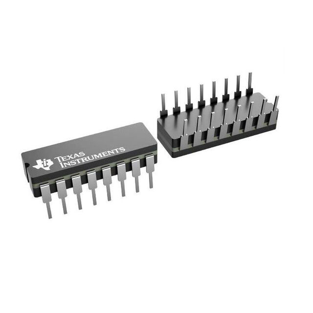
CD54HCT174F
ActiveHIGH SPEED CMOS LOGIC HEX D-TYPE FLIP-FLOPS WITH RESET
Deep-Dive with AI
Search across all available documentation for this part.

CD54HCT174F
ActiveHIGH SPEED CMOS LOGIC HEX D-TYPE FLIP-FLOPS WITH RESET
Deep-Dive with AI
Technical Specifications
Parameters and characteristics for this part
| Specification | CD54HCT174F |
|---|---|
| Clock Frequency | 25 MHz |
| Current - Output High, Low | 4 mA, 4 mA |
| Current - Quiescent (Iq) | 8 ÁA |
| Input Capacitance | 10 pF |
| Max Propagation Delay @ V, Max CL | 40 ns |
| Mounting Type | Through Hole |
| Number of Bits per Element | 6 |
| Number of Elements [custom] | 1 |
| Operating Temperature [Max] | 125 °C |
| Operating Temperature [Min] | -55 C |
| Output Type | Non-Inverted |
| Package / Case | 16-CDIP (0.300", 7.62mm) |
| Supplier Device Package | 16-CDIP |
| Trigger Type | Positive Edge |
| Type | D-Type |
| Voltage - Supply [Max] | 5.5 V |
| Voltage - Supply [Min] | 4.5 V |
Pricing
Prices provided here are for design reference only. For realtime values and availability, please visit the distributors directly
CD54HCT174 Series
High Speed CMOS Logic Hex D-Type Flip-Flops with Reset
| Part | Output Type | Trigger Type | Current - Quiescent (Iq) | Number of Bits per Element | Max Propagation Delay @ V, Max CL | Current - Output High, Low | Type | Package / Case | Operating Temperature [Min] | Operating Temperature [Max] | Clock Frequency | Number of Elements [custom] | Supplier Device Package | Input Capacitance | Mounting Type | Voltage - Supply [Max] | Voltage - Supply [Min] |
|---|---|---|---|---|---|---|---|---|---|---|---|---|---|---|---|---|---|
Texas Instruments CD54HCT174FThe ’HC174 and ’HCT174 are edge triggered flip-flops which utilize silicon gate CMOS circuitry to implement D-type flip-flops. They possess low power and speeds comparable to low power Schottky TTL circuits. The devices contain six master-slave flip-flops with a common clock and common reset. Data on the D input having the specified setup and hold times is transferred to the Q output on the low to high transition of the CLOCK input. The MR\ input, when low, sets all outputs to a low state.
Each output can drive ten low power Schottky TTL equivalent loads. The ’HCT174 is functional as well as, pin compatible to the ’LS174.
The ’HC174 and ’HCT174 are edge triggered flip-flops which utilize silicon gate CMOS circuitry to implement D-type flip-flops. They possess low power and speeds comparable to low power Schottky TTL circuits. The devices contain six master-slave flip-flops with a common clock and common reset. Data on the D input having the specified setup and hold times is transferred to the Q output on the low to high transition of the CLOCK input. The MR\ input, when low, sets all outputs to a low state.
Each output can drive ten low power Schottky TTL equivalent loads. The ’HCT174 is functional as well as, pin compatible to the ’LS174. | Non-Inverted | Positive Edge | 8 ÁA | 6 | 40 ns | 4 mA, 4 mA | D-Type | 16-CDIP (0.300", 7.62mm) | -55 C | 125 °C | 25 MHz | 1 | 16-CDIP | 10 pF | Through Hole | 5.5 V | 4.5 V |
Description
General part information
CD54HCT174 Series
The ’HC174 and ’HCT174 are edge triggered flip-flops which utilize silicon gate CMOS circuitry to implement D-type flip-flops. They possess low power and speeds comparable to low power Schottky TTL circuits. The devices contain six master-slave flip-flops with a common clock and common reset. Data on the D input having the specified setup and hold times is transferred to the Q output on the low to high transition of the CLOCK input. The MR\ input, when low, sets all outputs to a low state.
Each output can drive ten low power Schottky TTL equivalent loads. The ’HCT174 is functional as well as, pin compatible to the ’LS174.
The ’HC174 and ’HCT174 are edge triggered flip-flops which utilize silicon gate CMOS circuitry to implement D-type flip-flops. They possess low power and speeds comparable to low power Schottky TTL circuits. The devices contain six master-slave flip-flops with a common clock and common reset. Data on the D input having the specified setup and hold times is transferred to the Q output on the low to high transition of the CLOCK input. The MR\ input, when low, sets all outputs to a low state.
Documents
Technical documentation and resources


