


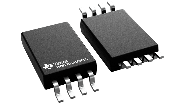
CDCS501PW
ActiveCLOCK DRIVER WITH OPTIONAL SPREAD-SPECTRUM CLOCKING
CDCS501PW
ActiveCLOCK DRIVER WITH OPTIONAL SPREAD-SPECTRUM CLOCKING
Description
General part information
CDCS501 Series
The CDCS501 is a spread spectrum capable, LVCMOS Input Clock Buffer for EMI reduction.
The device is designed to counter common EMI problems in modern electronic designs.
It accepts a 3.3V LVCMOS signal at the input and spread this signal by a small amount, centered around the input frequency. The amount of spread can be selected via 3 control pins. The Functional Table contains detailed information on the amount of spread. A 4th control pin can be used to activate or deactivate the Spread Spectrum Clock Generator.
Technical Specifications
Parameters and characteristics for this part
| Specification | CDCS501PW |
|---|---|
| Differential Input | No |
| Differential Output | No |
| Divider | No |
| Frequency - Max | 108 MHz |
| Input | LVCMOS |
| Input Ratio | 1 |
| Mounting Type | Surface Mount |
| Multiplier | No |
| Number of Circuits | 1 |
| Operating Temperature (Max) | 85 °C |
| Operating Temperature (Min) | -40 °C |
| Output | LVCMOS |
| Output Ratio | 1 |
| Package Length | 0.173 in |
| Package Name | 8-TSSOP |
| Package Width | 4.4 mm |
| PLL | No |
| Type | Spread Spectrum Clock Driver |
| Voltage - Supply (Maximum) | 3.6 V |
| Voltage - Supply (Minimum) | 3 V |
Pricing
Prices provided here are for design reference only. For realtime values and availability, please visit the distributors directly
Sign in to see pricing
Create a free account to access distributor pricing data.
CAD
3D models and CAD resources for this part
Documents
Technical documentation and resources

