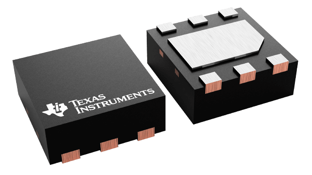
TPS61170QDRVRQ1
Active3-V TO 18-V WIDE INPUT RANGE, 1.2-A BOOST CONVERTER IN 2-MM X 2-MM QFN PACKAGE, AEC-Q100 QUALIFIED
Deep-Dive with AI
Search across all available documentation for this part.

TPS61170QDRVRQ1
Active3-V TO 18-V WIDE INPUT RANGE, 1.2-A BOOST CONVERTER IN 2-MM X 2-MM QFN PACKAGE, AEC-Q100 QUALIFIED
Technical Specifications
Parameters and characteristics commom to parts in this series
| Specification | TPS61170QDRVRQ1 | TPS61170 Series |
|---|---|---|
| Board Type | - | Fully Populated |
| Current - Output | 960 mA | 420 - 960 mA |
| Frequency - Switching | 1.2 MHz | 1.2 MHz |
| Function | Step-Up, Step-Up/Step-Down | Step-Up, Step-Up/Step-Down |
| Grade | Automotive | Automotive |
| Main Purpose | - | DC/DC, Step Up, DC/DC, Step Up or Down |
| Mounting Type | Surface Mount | Surface Mount |
| Number of Outputs | 1 | 1 |
| Operating Temperature [Max] | 125 °C | 85 - 125 °C |
| Operating Temperature [Min] | -40 °C | -40 °C |
| Output Configuration | Positive | Positive |
| Output Type | Adjustable | Adjustable |
| Outputs and Type | - | Non-Isolated |
| Outputs and Type | - | 1 |
| Qualification | AEC-Q100 | AEC-Q100 |
| Regulator Topology | - | Boost, Buck-Boost |
| Supplied Contents | - | Board(s) |
| Supplier Device Package | 6-WSON (2x2) | 6-WSON (2x2) |
| Synchronous Rectifier | False | False |
| Topology | Buck-Boost, SEPIC, Flyback, Boost | Buck-Boost, SEPIC, Flyback, Boost |
| Utilized IC / Part | - | TPS61170 |
| Voltage - Input | - | 9 VDC |
| Voltage - Input | - | 15 - 18 V |
| Voltage - Input (Max) [Max] | 18 V | 18 V |
| Voltage - Input (Min) [Min] | 3 V | 3 V |
| Voltage - Output | - | 12 - 24 V |
| Voltage - Output (Max) | 38 V | 38 V |
Pricing
Prices provided here are for design reference only. For realtime values and availability, please visit the distributors directly
| Distributor | Package | Quantity | $ | |
|---|---|---|---|---|
| Digikey | Cut Tape (CT) | 1 | $ 2.71 | |
| 10 | $ 2.44 | |||
| 25 | $ 2.30 | |||
| 100 | $ 1.96 | |||
| 250 | $ 1.84 | |||
| 500 | $ 1.61 | |||
| 1000 | $ 1.33 | |||
| Digi-Reel® | 1 | $ 2.71 | ||
| 10 | $ 2.44 | |||
| 25 | $ 2.30 | |||
| 100 | $ 1.96 | |||
| 250 | $ 1.84 | |||
| 500 | $ 1.61 | |||
| 1000 | $ 1.33 | |||
| Tape & Reel (TR) | 3000 | $ 1.24 | ||
| 6000 | $ 1.19 | |||
| Newark | Each (Supplied on Cut Tape) | 1 | $ 3.31 | |
| 10 | $ 3.16 | |||
| 25 | $ 3.01 | |||
| 50 | $ 2.87 | |||
| 100 | $ 2.75 | |||
| 250 | $ 2.66 | |||
| 500 | $ 2.60 | |||
| 1000 | $ 2.56 | |||
| Texas Instruments | LARGE T&R | 1 | $ 2.04 | |
| 100 | $ 1.68 | |||
| 250 | $ 1.21 | |||
| 1000 | $ 0.91 | |||
TPS61170 Series
1.2A SWITCH, 38V HIGH VOLTAGE BOOST CONVERTER IN 2X2MM QFN PACKAGE
| Part | Voltage - Input (Min) [Min] | Function | Mounting Type | Synchronous Rectifier | Operating Temperature [Max] | Operating Temperature [Min] | Voltage - Output (Max) | Topology | Frequency - Switching | Voltage - Input (Max) [Max] | Output Configuration | Current - Output | Number of Outputs | Output Type | Supplier Device Package | Qualification | Grade | Supplied Contents | Outputs and Type | Outputs and Type | Voltage - Input [Min] | Voltage - Input [Max] | Regulator Topology | Utilized IC / Part | Voltage - Output | Main Purpose | Board Type |
|---|---|---|---|---|---|---|---|---|---|---|---|---|---|---|---|---|---|---|---|---|---|---|---|---|---|---|---|
Texas Instruments TPS61170DRVT | 3 V | Step-Up, Step-Up/Step-Down | Surface Mount | 85 °C | -40 °C | 38 V | Boost, Buck-Boost, Flyback, SEPIC | 1.2 MHz | 18 V | Positive | 960 mA | 1 | Adjustable | 6-WSON (2x2) | |||||||||||||
Texas Instruments TPS61170QDRVRQ1 | 3 V | Step-Up, Step-Up/Step-Down | Surface Mount | 125 °C | -40 °C | 38 V | Boost, Buck-Boost, Flyback, SEPIC | 1.2 MHz | 18 V | Positive | 960 mA | 1 | Adjustable | 6-WSON (2x2) | AEC-Q100 | Automotive | |||||||||||
Texas Instruments TPS61170EVM-280 | 1.2 MHz | 550 mA | Board(s) | Non-Isolated | 1 | 9 VDC | 18 V | Boost | TPS61170 | 24 V | DC/DC, Step Up | Fully Populated | |||||||||||||||
Texas Instruments TPS61170DRVRG4 | 3 V | Step-Up, Step-Up/Step-Down | Surface Mount | 85 °C | -40 °C | 38 V | Boost, Buck-Boost, Flyback, SEPIC | 1.2 MHz | 18 V | Positive | 960 mA | 1 | Adjustable | 6-WSON (2x2) | |||||||||||||
Texas Instruments TPS61170EVM-316 | 1.2 MHz | 420 mA | Board(s) | Non-Isolated | 1 | 9 VDC | 15 V | Buck-Boost | TPS61170 | 12 V | DC/DC, Step Up or Down | Fully Populated |
Description
General part information
TPS61170 Series
The TPS61170-Q1 is a monolithic, high-voltage switching regulator with integrated 1.2-A, 40-V power MOSFET. The device can be configured in several standard switching-regulator topologies, including boost and SEPIC. The device has a wide input-voltage range to support applications with input voltage from multicell batteries or regulated 5-V, 12-V power rails.
The TPS61170-Q1 operates at a 1.2-MHz switching frequency, allowing the use of low-profile inductors and low-value ceramic input and output capacitors. External loop compensation components give the user flexibility to optimize loop compensation and transient response. The device has built-in protection features, such as pulse-by-pulse overcurrent limit, soft start, and thermal shutdown.
The FB pin regulates to a reference voltage of1.229 V. The reference voltage can be lowered using a 1-wire digital interface (EasyScale™ protocol) through the CTRL pin. Alternatively, a pulse width-modulation (PWM) signal can be applied to the CTRL pin. The duty cycle of the signal reduces the feedback reference voltage proportionally.
Documents
Technical documentation and resources


