SN75LP1185DW
ActiveLOW-POWER MULTIPLE RS-232 DRIVERS AND RECEIVERS
Deep-Dive with AI
Search across all available documentation for this part.
SN75LP1185DW
ActiveLOW-POWER MULTIPLE RS-232 DRIVERS AND RECEIVERS
Deep-Dive with AI
Technical Specifications
Parameters and characteristics commom to parts in this series
| Specification | SN75LP1185DW | SN75LP1185 Series |
|---|---|---|
| Duplex | Full | Full |
| Mounting Type | Surface Mount | Surface Mount |
| Number of Drivers/Receivers [custom] | 5 | 5 |
| Number of Drivers/Receivers [custom] | 3 | 3 |
| Operating Temperature [Max] | 70 ░C | 70 ░C |
| Operating Temperature [Min] | 0 °C | 0 °C |
| Package / Case | 7.5 mm, 0.295 in | 0.209 - 7.5 mm |
| Package / Case | 20-SOIC | 20-SOIC, 20-SSOP |
| Protocol | RS232 | RS232 |
| Receiver Hysteresis | 1 V | 1 V |
| Supplier Device Package | 20-SOIC | 20-SOIC, 20-SSOP |
| Type | Transceiver | Transceiver |
| Voltage - Supply [Max] | 5.25 V | 5.25 V |
| Voltage - Supply [Min] | 4.75 V | 4.75 V |
Pricing
Prices provided here are for design reference only. For realtime values and availability, please visit the distributors directly
SN75LP1185 Series
Low-Power Multiple RS-232 Drivers and Receivers
| Part | Package / Case | Package / Case | Protocol | Receiver Hysteresis | Supplier Device Package | Number of Drivers/Receivers [custom] | Number of Drivers/Receivers [custom] | Mounting Type | Voltage - Supply [Min] | Voltage - Supply [Max] | Operating Temperature [Max] | Operating Temperature [Min] | Duplex | Type |
|---|---|---|---|---|---|---|---|---|---|---|---|---|---|---|
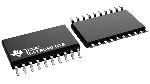
Texas Instruments SN75LP1185DWThe SN75LP1185 is a low-power bipolar device containing three drivers and five receivers, with 15 kV of ESD protection on the bus pins with respect to each other. Bus pins are defined as those pins that tie directly to the serial-port connector, including GND. The pinout matches the flow-through design of the industry-standard SN75185 and SN75C185. The flow-through pinout of the SN75LP1185 allows easy interconnection of the UART and serial-port connector of the IBM PC/AT and compatibles. The SN75LP1185 provides a rugged, low-cost solution for this function with the combination of the bipolar processing and 15 kV of ESD protection.
The SN75LP1185 has internal slew-rate control to provide a maximum rate of change in the output signal of 30 V/us. The driver output swing is nominally clamped at ±6 V to enable the higher data rates associated with this device and to reduce EMI emissions. Even though the driver outputs are clamped, they can handle voltages up to ±15 V without damage. All the logic inputs can accept 3.3-V or 5-V input signals.
The SN75LP1185 complies with the requirements of TIA/EIA-232-F and ITU V.28. These standards are for data interchange between a host computer and peripheral at signaling rates up to 20 kbit/s. The switching speeds of the SN75LP1185 support rates up to 256 kbit/s.
The SN75LP1185 is characterized for operation from 0°C to 70°C.
The SN75LP1185 is a low-power bipolar device containing three drivers and five receivers, with 15 kV of ESD protection on the bus pins with respect to each other. Bus pins are defined as those pins that tie directly to the serial-port connector, including GND. The pinout matches the flow-through design of the industry-standard SN75185 and SN75C185. The flow-through pinout of the SN75LP1185 allows easy interconnection of the UART and serial-port connector of the IBM PC/AT and compatibles. The SN75LP1185 provides a rugged, low-cost solution for this function with the combination of the bipolar processing and 15 kV of ESD protection.
The SN75LP1185 has internal slew-rate control to provide a maximum rate of change in the output signal of 30 V/us. The driver output swing is nominally clamped at ±6 V to enable the higher data rates associated with this device and to reduce EMI emissions. Even though the driver outputs are clamped, they can handle voltages up to ±15 V without damage. All the logic inputs can accept 3.3-V or 5-V input signals.
The SN75LP1185 complies with the requirements of TIA/EIA-232-F and ITU V.28. These standards are for data interchange between a host computer and peripheral at signaling rates up to 20 kbit/s. The switching speeds of the SN75LP1185 support rates up to 256 kbit/s.
The SN75LP1185 is characterized for operation from 0°C to 70°C. | 0.295 in, 7.5 mm | 20-SOIC | RS232 | 1 V | 20-SOIC | 5 | 3 | Surface Mount | 4.75 V | 5.25 V | 70 ░C | 0 °C | Full | Transceiver |
Texas Instruments SN75LP1185DWRThe SN75LP1185 is a low-power bipolar device containing three drivers and five receivers, with 15 kV of ESD protection on the bus pins with respect to each other. Bus pins are defined as those pins that tie directly to the serial-port connector, including GND. The pinout matches the flow-through design of the industry-standard SN75185 and SN75C185. The flow-through pinout of the SN75LP1185 allows easy interconnection of the UART and serial-port connector of the IBM PC/AT and compatibles. The SN75LP1185 provides a rugged, low-cost solution for this function with the combination of the bipolar processing and 15 kV of ESD protection.
The SN75LP1185 has internal slew-rate control to provide a maximum rate of change in the output signal of 30 V/us. The driver output swing is nominally clamped at ±6 V to enable the higher data rates associated with this device and to reduce EMI emissions. Even though the driver outputs are clamped, they can handle voltages up to ±15 V without damage. All the logic inputs can accept 3.3-V or 5-V input signals.
The SN75LP1185 complies with the requirements of TIA/EIA-232-F and ITU V.28. These standards are for data interchange between a host computer and peripheral at signaling rates up to 20 kbit/s. The switching speeds of the SN75LP1185 support rates up to 256 kbit/s.
The SN75LP1185 is characterized for operation from 0°C to 70°C.
The SN75LP1185 is a low-power bipolar device containing three drivers and five receivers, with 15 kV of ESD protection on the bus pins with respect to each other. Bus pins are defined as those pins that tie directly to the serial-port connector, including GND. The pinout matches the flow-through design of the industry-standard SN75185 and SN75C185. The flow-through pinout of the SN75LP1185 allows easy interconnection of the UART and serial-port connector of the IBM PC/AT and compatibles. The SN75LP1185 provides a rugged, low-cost solution for this function with the combination of the bipolar processing and 15 kV of ESD protection.
The SN75LP1185 has internal slew-rate control to provide a maximum rate of change in the output signal of 30 V/us. The driver output swing is nominally clamped at ±6 V to enable the higher data rates associated with this device and to reduce EMI emissions. Even though the driver outputs are clamped, they can handle voltages up to ±15 V without damage. All the logic inputs can accept 3.3-V or 5-V input signals.
The SN75LP1185 complies with the requirements of TIA/EIA-232-F and ITU V.28. These standards are for data interchange between a host computer and peripheral at signaling rates up to 20 kbit/s. The switching speeds of the SN75LP1185 support rates up to 256 kbit/s.
The SN75LP1185 is characterized for operation from 0°C to 70°C. | 0.295 in, 7.5 mm | 20-SOIC | RS232 | 1 V | 20-SOIC | 5 | 3 | Surface Mount | 4.75 V | 5.25 V | 70 ░C | 0 °C | Full | Transceiver |
Texas Instruments SN75LP1185DBRThe SN75LP1185 is a low-power bipolar device containing three drivers and five receivers, with 15 kV of ESD protection on the bus pins with respect to each other. Bus pins are defined as those pins that tie directly to the serial-port connector, including GND. The pinout matches the flow-through design of the industry-standard SN75185 and SN75C185. The flow-through pinout of the SN75LP1185 allows easy interconnection of the UART and serial-port connector of the IBM PC/AT and compatibles. The SN75LP1185 provides a rugged, low-cost solution for this function with the combination of the bipolar processing and 15 kV of ESD protection.
The SN75LP1185 has internal slew-rate control to provide a maximum rate of change in the output signal of 30 V/us. The driver output swing is nominally clamped at ±6 V to enable the higher data rates associated with this device and to reduce EMI emissions. Even though the driver outputs are clamped, they can handle voltages up to ±15 V without damage. All the logic inputs can accept 3.3-V or 5-V input signals.
The SN75LP1185 complies with the requirements of TIA/EIA-232-F and ITU V.28. These standards are for data interchange between a host computer and peripheral at signaling rates up to 20 kbit/s. The switching speeds of the SN75LP1185 support rates up to 256 kbit/s.
The SN75LP1185 is characterized for operation from 0°C to 70°C.
The SN75LP1185 is a low-power bipolar device containing three drivers and five receivers, with 15 kV of ESD protection on the bus pins with respect to each other. Bus pins are defined as those pins that tie directly to the serial-port connector, including GND. The pinout matches the flow-through design of the industry-standard SN75185 and SN75C185. The flow-through pinout of the SN75LP1185 allows easy interconnection of the UART and serial-port connector of the IBM PC/AT and compatibles. The SN75LP1185 provides a rugged, low-cost solution for this function with the combination of the bipolar processing and 15 kV of ESD protection.
The SN75LP1185 has internal slew-rate control to provide a maximum rate of change in the output signal of 30 V/us. The driver output swing is nominally clamped at ±6 V to enable the higher data rates associated with this device and to reduce EMI emissions. Even though the driver outputs are clamped, they can handle voltages up to ±15 V without damage. All the logic inputs can accept 3.3-V or 5-V input signals.
The SN75LP1185 complies with the requirements of TIA/EIA-232-F and ITU V.28. These standards are for data interchange between a host computer and peripheral at signaling rates up to 20 kbit/s. The switching speeds of the SN75LP1185 support rates up to 256 kbit/s.
The SN75LP1185 is characterized for operation from 0°C to 70°C. | 0.209 in, 5.3 mm | 20-SSOP | RS232 | 1 V | 20-SSOP | 5 | 3 | Surface Mount | 4.75 V | 5.25 V | 70 ░C | 0 °C | Full | Transceiver |
Description
General part information
SN75LP1185 Series
The SN75LP1185 is a low-power bipolar device containing three drivers and five receivers, with 15 kV of ESD protection on the bus pins with respect to each other. Bus pins are defined as those pins that tie directly to the serial-port connector, including GND. The pinout matches the flow-through design of the industry-standard SN75185 and SN75C185. The flow-through pinout of the SN75LP1185 allows easy interconnection of the UART and serial-port connector of the IBM PC/AT and compatibles. The SN75LP1185 provides a rugged, low-cost solution for this function with the combination of the bipolar processing and 15 kV of ESD protection.
The SN75LP1185 has internal slew-rate control to provide a maximum rate of change in the output signal of 30 V/us. The driver output swing is nominally clamped at ±6 V to enable the higher data rates associated with this device and to reduce EMI emissions. Even though the driver outputs are clamped, they can handle voltages up to ±15 V without damage. All the logic inputs can accept 3.3-V or 5-V input signals.
The SN75LP1185 complies with the requirements of TIA/EIA-232-F and ITU V.28. These standards are for data interchange between a host computer and peripheral at signaling rates up to 20 kbit/s. The switching speeds of the SN75LP1185 support rates up to 256 kbit/s.
Documents
Technical documentation and resources