


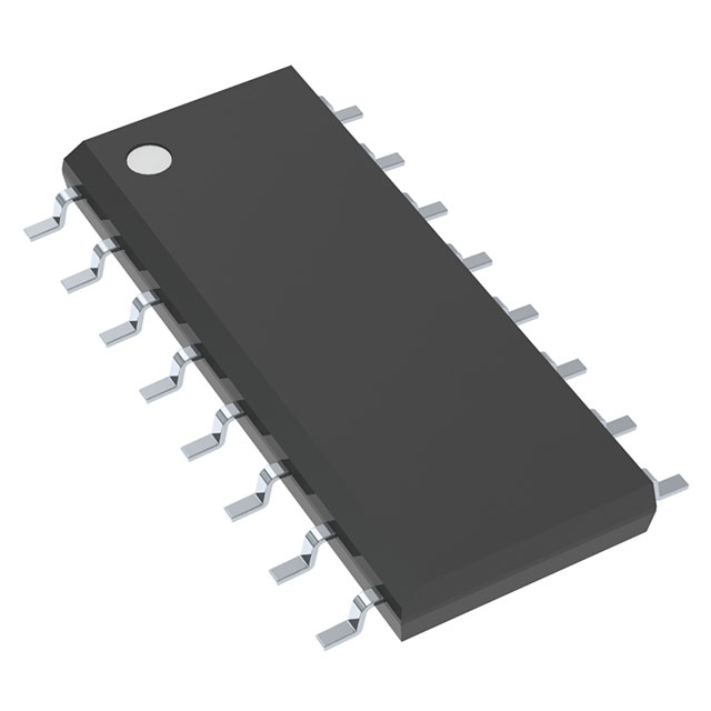
SN74LS173ADR
ObsoleteIC FF D-TYPE SNGL 4BIT 16SOIC
SN74LS173ADR
ObsoleteIC FF D-TYPE SNGL 4BIT 16SOIC
Description
General part information
74LS173 Series
The '173 and 'LS173A 4-bit registers include D-type flip-flops featuring totem-pole 3-state outputs capable of driving highly capacitiveor relatively low-impedance loads. The high-impedance third state and increased high-logic-level drive provide these flip-flops with the capability of being connected directly to and driving the bus lines in a bus-organized system without need for interface or pull-up components. Up to 128 of the SN74173 or SN74LS173A outputs can be connected to a common bus and still drive two Series 54/74 or 54LS/74LS TTL normalized loads, respectively. Similarly, up to 49 of the SN54173 or SN54LS173A outputs can be connected to a common bus and drive one additional Series 54/74 or 54LS/74LS TTL normalized load, respectively. To minimize the possibility that two outputs will attempt to take a common bus to opposite logic levels, the output control circuitry is designed so that the average output disable times are shorter than the average output enable times.
Gated enable inputs are provided on these devices for controlling the entry of data into the flip-flops. When both data-enable (G\1, G\2) inputs are low, data at the D inputs are loaded into their respective flip-flops on the next positive transition of the buffered clock input. Gate output-control (M, N) inputs also are provided. When both are low, the normal logic states (high or low levels) of the four outputs are available for driving the loads or bus lines. The outputs are disabled independently from the level of the clock by a high logic level at either output-control input. The outputs then present a high impedance and neither load nor drive the bus line. Detailed operation is given in the function table.
The SN54173 and SN54LS173A are characterized for operation over the full military temperature range of -55°C to 125°C. The SN74173 and SN74LS173A are characterized for operation from 0°C to 70°C.
Technical Specifications
Parameters and characteristics for this part
| Specification | SN74LS173ADR |
|---|---|
| Clock Frequency | 50 MHz |
| Current - Output High | 2.6 mA |
| Current - Output Low | 24 mA |
| Current - Quiescent (Iq) | 24 mA |
| Function | Master Reset |
| Max CL | 45 pF |
| Max Propagation Delay | 25 ns |
| Mounting Type | Surface Mount |
| Number of Bits per Element | 4 bits |
| Number of Elements | 1 |
| Operating Temperature (Max) | 70 °C |
| Operating Temperature (Min) | 0 °C |
| Output Type | Tri-State, Non-Inverted |
| Package Length | 0.154 in |
| Package Name | 16-SOIC |
| Package Width | 3.9 mm |
| Trigger Type | Positive Edge |
| Type | D-Type |
| Voltage - Supply (Maximum) | 5.25 V |
| Voltage - Supply (Minimum) | 4.75 V |
Pricing
Prices provided here are for design reference only. For realtime values and availability, please visit the distributors directly
Sign in to see pricing
Create a free account to access distributor pricing data.
CAD
3D models and CAD resources for this part
Documents
Technical documentation and resources
No documents available


