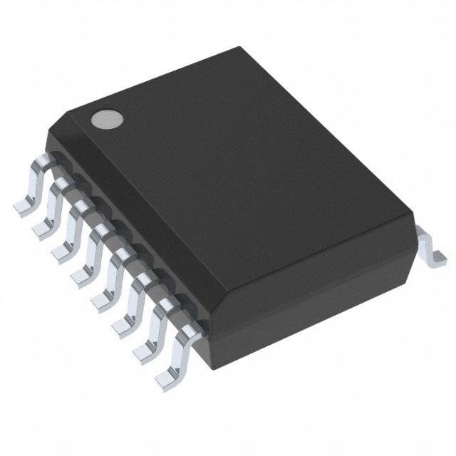
ADC12130CIWM/NOPB
ActiveSELF-CALIBRATING 12-BIT PLUS SIGN SERIAL I/O A/D CONVERTER WITH 2-CHANNEL MUX AND SAMPLE/HOLD
Deep-Dive with AI
Search across all available documentation for this part.

ADC12130CIWM/NOPB
ActiveSELF-CALIBRATING 12-BIT PLUS SIGN SERIAL I/O A/D CONVERTER WITH 2-CHANNEL MUX AND SAMPLE/HOLD
Deep-Dive with AI
Technical Specifications
Parameters and characteristics commom to parts in this series
| Specification | ADC12130CIWM/NOPB | ADC12130 Series |
|---|---|---|
| Architecture | SAR | SAR |
| Configuration | MUX-S/H-ADC | MUX-S/H-ADC |
| Data Interface | SPI | SPI |
| Input Type | Single Ended, Differential, Pseudo-Differential | Single Ended, Differential, Pseudo-Differential |
| Mounting Type | Surface Mount | Surface Mount |
| Number of A/D Converters | 1 | 1 |
| Number of Bits | 12 | 12 |
| Number of Inputs | 1, 2 | 1 - 2 |
| Operating Temperature [Max] | 85 °C | 85 °C |
| Operating Temperature [Min] | -40 °C | -40 °C |
| Package / Case | 16-SOIC | 16-SOIC |
| Ratio - S/H:ADC | 1:1 | 1:1 |
| Reference Type | External | External |
| Sampling Rate (Per Second) | 114k | 114k |
| Supplier Device Package | 16-SOIC | 16-SOIC |
| Voltage - Supply, Analog [Max] | 5.5 V | 5.5 V |
| Voltage - Supply, Analog [Min] | 3 V | 3 V |
| Voltage - Supply, Digital [Max] | 5.5 V | 5.5 V |
| Voltage - Supply, Digital [Min] | 3 V | 3 V |
Pricing
Prices provided here are for design reference only. For realtime values and availability, please visit the distributors directly
ADC12130 Series
Self-calibrating 12-bit plus sign serial I/O A/D converter with 2-channel MUX and sample/hold
| Part | Configuration | Supplier Device Package | Voltage - Supply, Analog [Min] | Voltage - Supply, Analog [Max] | Number of A/D Converters | Sampling Rate (Per Second) | Package / Case | Ratio - S/H:ADC | Architecture | Data Interface | Number of Inputs | Number of Bits | Reference Type | Mounting Type | Operating Temperature [Min] | Operating Temperature [Max] | Input Type | Voltage - Supply, Digital [Max] | Voltage - Supply, Digital [Min] |
|---|---|---|---|---|---|---|---|---|---|---|---|---|---|---|---|---|---|---|---|
Texas Instruments ADC12130CIWM/NOPBNOTE: Some device/package combinations are obsolete and are described and shown here for reference only. See our web site for product availability.
The ADC12130, ADC12132 and ADC12138 are 12-bit plus sign successive approximation Analog-to-Digital converters with serial I/O and configurable input multiplexer. The ADC12132 and ADC12138 have a 2 and an 8 channel multiplexer, respectively. The differential multiplexer outputs and ADC inputs are available on the MUXOUT1, MUXOUT2, A/DIN1 and A/DIN2 pins. The ADC12130 has a two channel multiplexer with the multiplexer outputs and ADC inputs internally connected. The ADC12130 family is tested and specified with a 5 MHz clock. On request, these ADCs go through a self calibration process that adjusts linearity, zero and full-scale errors to typically less than ±1 LSB each.
The analog inputs can be configured to operate in various combinations of single-ended, differential, or pseudo-differential modes. A fully differential unipolar analog input range (0V to +5V) can be accommodated with a single +5V supply. In the differential modes, valid outputs are obtained even when the negative inputs are greater than the positive because of the 12-bit plus sign output data format.
The serial I/O is configured to comply with NSC MICROWIRE. For voltage references, see the LM4040, LM4050 or LM4041.
NOTE: Some device/package combinations are obsolete and are described and shown here for reference only. See our web site for product availability.
The ADC12130, ADC12132 and ADC12138 are 12-bit plus sign successive approximation Analog-to-Digital converters with serial I/O and configurable input multiplexer. The ADC12132 and ADC12138 have a 2 and an 8 channel multiplexer, respectively. The differential multiplexer outputs and ADC inputs are available on the MUXOUT1, MUXOUT2, A/DIN1 and A/DIN2 pins. The ADC12130 has a two channel multiplexer with the multiplexer outputs and ADC inputs internally connected. The ADC12130 family is tested and specified with a 5 MHz clock. On request, these ADCs go through a self calibration process that adjusts linearity, zero and full-scale errors to typically less than ±1 LSB each.
The analog inputs can be configured to operate in various combinations of single-ended, differential, or pseudo-differential modes. A fully differential unipolar analog input range (0V to +5V) can be accommodated with a single +5V supply. In the differential modes, valid outputs are obtained even when the negative inputs are greater than the positive because of the 12-bit plus sign output data format.
The serial I/O is configured to comply with NSC MICROWIRE. For voltage references, see the LM4040, LM4050 or LM4041. | MUX-S/H-ADC | 16-SOIC | 3 V | 5.5 V | 1 | 114k | 16-SOIC | 1:1 | SAR | SPI | 1, 2 | 12 | External | Surface Mount | -40 °C | 85 °C | Differential, Pseudo-Differential, Single Ended | 5.5 V | 3 V |
Texas Instruments ADC12130CIWMX/NOPBNOTE: Some device/package combinations are obsolete and are described and shown here for reference only. See our web site for product availability.
The ADC12130, ADC12132 and ADC12138 are 12-bit plus sign successive approximation Analog-to-Digital converters with serial I/O and configurable input multiplexer. The ADC12132 and ADC12138 have a 2 and an 8 channel multiplexer, respectively. The differential multiplexer outputs and ADC inputs are available on the MUXOUT1, MUXOUT2, A/DIN1 and A/DIN2 pins. The ADC12130 has a two channel multiplexer with the multiplexer outputs and ADC inputs internally connected. The ADC12130 family is tested and specified with a 5 MHz clock. On request, these ADCs go through a self calibration process that adjusts linearity, zero and full-scale errors to typically less than ±1 LSB each.
The analog inputs can be configured to operate in various combinations of single-ended, differential, or pseudo-differential modes. A fully differential unipolar analog input range (0V to +5V) can be accommodated with a single +5V supply. In the differential modes, valid outputs are obtained even when the negative inputs are greater than the positive because of the 12-bit plus sign output data format.
The serial I/O is configured to comply with NSC MICROWIRE. For voltage references, see the LM4040, LM4050 or LM4041.
NOTE: Some device/package combinations are obsolete and are described and shown here for reference only. See our web site for product availability.
The ADC12130, ADC12132 and ADC12138 are 12-bit plus sign successive approximation Analog-to-Digital converters with serial I/O and configurable input multiplexer. The ADC12132 and ADC12138 have a 2 and an 8 channel multiplexer, respectively. The differential multiplexer outputs and ADC inputs are available on the MUXOUT1, MUXOUT2, A/DIN1 and A/DIN2 pins. The ADC12130 has a two channel multiplexer with the multiplexer outputs and ADC inputs internally connected. The ADC12130 family is tested and specified with a 5 MHz clock. On request, these ADCs go through a self calibration process that adjusts linearity, zero and full-scale errors to typically less than ±1 LSB each.
The analog inputs can be configured to operate in various combinations of single-ended, differential, or pseudo-differential modes. A fully differential unipolar analog input range (0V to +5V) can be accommodated with a single +5V supply. In the differential modes, valid outputs are obtained even when the negative inputs are greater than the positive because of the 12-bit plus sign output data format.
The serial I/O is configured to comply with NSC MICROWIRE. For voltage references, see the LM4040, LM4050 or LM4041. | MUX-S/H-ADC | 16-SOIC | 3 V | 5.5 V | 1 | 114k | 16-SOIC | 1:1 | SAR | SPI | 1, 2 | 12 | External | Surface Mount | -40 °C | 85 °C | Differential, Pseudo-Differential, Single Ended | 5.5 V | 3 V |
Description
General part information
ADC12130 Series
NOTE: Some device/package combinations are obsolete and are described and shown here for reference only. See our web site for product availability.
The ADC12130, ADC12132 and ADC12138 are 12-bit plus sign successive approximation Analog-to-Digital converters with serial I/O and configurable input multiplexer. The ADC12132 and ADC12138 have a 2 and an 8 channel multiplexer, respectively. The differential multiplexer outputs and ADC inputs are available on the MUXOUT1, MUXOUT2, A/DIN1 and A/DIN2 pins. The ADC12130 has a two channel multiplexer with the multiplexer outputs and ADC inputs internally connected. The ADC12130 family is tested and specified with a 5 MHz clock. On request, these ADCs go through a self calibration process that adjusts linearity, zero and full-scale errors to typically less than ±1 LSB each.
The analog inputs can be configured to operate in various combinations of single-ended, differential, or pseudo-differential modes. A fully differential unipolar analog input range (0V to +5V) can be accommodated with a single +5V supply. In the differential modes, valid outputs are obtained even when the negative inputs are greater than the positive because of the 12-bit plus sign output data format.
Documents
Technical documentation and resources


