


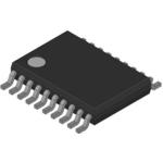
ADG5243FBRUZ
ActiveUSER DEFINED FAULT PROTECTION AND DETECTION, 0.8 PC QINJ, TRIPLE SPDT

ADG5243FBRUZ
ActiveUSER DEFINED FAULT PROTECTION AND DETECTION, 0.8 PC QINJ, TRIPLE SPDT
Description
General part information
ADG5243F Series
The ADG5243F comprises three independently selectable, singlepole/double-throw (SPDT) switches. All channels exhibit break-before-make switching action that prevents momentary shorting when switching channels. AnENinput enables or disables the device. When disabled, all channels are switched off. Each switch conducts equally well in both directions when on, and each switch has an input signal range that extends to the supplies. The primary supply voltages define the on-resistance profile, whereas the secondary supply voltages define the voltage level at which the overvoltage protection engages.When no power supplies are present, the channel remains in the off condition, and the switch inputs are high impedance. Under normal operating conditions, if the analog input signal levels on any Sx pin exceed the positive fault voltage (POSFV) or the negative fault voltage (NEGFV) by a threshold voltage (VT), the channel turns off and that Sx pin becomes high impedance. If the switch is selected to be on, then the drain pin is pulled to the secondary supply voltage that was exceeded. Input signal levels up to −55 V or +55 V relative to ground are blocked, in both the powered and unpowered conditions.The low capacitance and charge injection of these switches make them ideal solutions for data acquisition and sample-andhold applications, where low glitch switching and fast settling times are required.Note that, throughout this data sheet, multifunction pins, such as IN1/F1, are referred to either by the entire pin name or by a single function of the pin, for example, IN1, when only that function is relevant.PRODUCT HIGHLIGHTSThe source pins are protected against voltages greater than the secondary supply rails, up to −55 V and +55 V.The source pins are protected against voltages between −55 V and +55 V in an unpowered state.Overvoltage detection with the digital output indicates the operating state of the switches.Trench isolation guards against latch-up.Optimized for low charge injection and on-capacitance.The ADG5243F can be operated from a dual supply of ±5 V to ±22 V or a single power supply of 8 V to 44 V.APPLICATIONSAnalog input/output modulesProcess control/distributed control systemsData acquisitionInstrumentationAvionicsAutomatic test equipmentCommunication systemsRelay replacement
Technical Specifications
Parameters and characteristics for this part
| Specification | ADG5243FBRUZ |
|---|---|
| -3db Bandwidth | 350 MHz |
| Channel-to-Channel Matching (ΔRon) | 3 Ohm |
| Charge Injection | -1.4 pC |
| Crosstalk | -85 dB |
| Current - Leakage (Max) | 1 nA |
| Demultiplexer Outputs | 1 |
| Mounting Type | Surface Mount |
| Multiplexer Inputs | 2 |
| Number of Circuits | 3 |
| On-State Resistance (Max) | 335 Ohm |
| Operating Temperature (Max) | 125 °C |
| Operating Temperature (Min) | -40 °C |
| Package Length | 0.173 in |
| Package Name | 20-TSSOP |
| Package Width | 4.4 mm |
| Switch Circuit Type | SPDT |
| Switch Time Toff (Max) | 85 ns |
| Switch Time Ton (Max) | 215 ns |
| Voltage - Supply, Dual (Maximum) | 22 V |
| Voltage - Supply, Dual (Minimum) | -5 V |
| Voltage - Supply, Dual (Nominal) | 5 V |
| Voltage - Supply, Single (V+) (Maximum) | 44 V |
| Voltage - Supply, Single (V+) (Minimum) | 8 V |
Pricing
Prices provided here are for design reference only. For realtime values and availability, please visit the distributors directly
Sign in to see pricing
Create a free account to access distributor pricing data.
CAD
3D models and CAD resources for this part
Documents
Technical documentation and resources