ADC161S626 Series
16-Bit, 250-kSPS, 1-Ch SAR ADC with fully differential input
Manufacturer: Texas Instruments
Catalog
16-Bit, 250-kSPS, 1-Ch SAR ADC with fully differential input
Description
AI
The ADC161S626 is a 16-bit successive-approximation register (SAR) Analog-to-Digital converter (ADC) with a maximum sampling rate of 250 kSPS. The ADC161S626 has a minimum signal span accuracy of ±0.003% over the temperate range of –40°C to +85°C. The converter features a differential analog input with an excellent common-mode signal rejection ratio of 85 dB, making the ADC161S626 suitable for noisy environments.
The ADC161S626 operates with a single analog supply (VA) and a separate digital input/output (VIO) supply. VAcan range from 4.5 V to 5.5 V and VIOcan range from 2.7 V to 5.5 V. This allows a system designer to maximize performance and minimize power consumption by operating the analog portion of the ADC at a VAof 5 V while interfacing with a 3.3-V controller. The serial data output is binary 2’s complement and is SPI compatible.
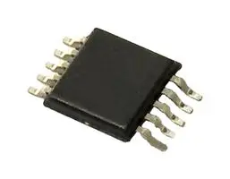
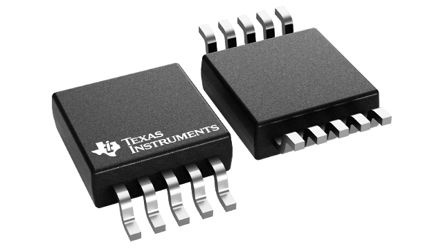
The performance of the ADC161S626 is ensured over temperature at clock rates of 1 MHz to 5 MHz and reference voltages of 2.5 V to 5.5 V. The ADC161S626 is available in a small 10-lead VSSOP package. The high accuracy, differential input, low power consumption, and small size make the ADC161S626 ideal for direct connection to bridge sensors and transducers in battery operated systems or remote data acquisition applications.
The ADC161S626 is a 16-bit successive-approximation register (SAR) Analog-to-Digital converter (ADC) with a maximum sampling rate of 250 kSPS. The ADC161S626 has a minimum signal span accuracy of ±0.003% over the temperate range of –40°C to +85°C. The converter features a differential analog input with an excellent common-mode signal rejection ratio of 85 dB, making the ADC161S626 suitable for noisy environments.
The ADC161S626 operates with a single analog supply (VA) and a separate digital input/output (VIO) supply. VAcan range from 4.5 V to 5.5 V and VIOcan range from 2.7 V to 5.5 V. This allows a system designer to maximize performance and minimize power consumption by operating the analog portion of the ADC at a VAof 5 V while interfacing with a 3.3-V controller. The serial data output is binary 2’s complement and is SPI compatible.
The performance of the ADC161S626 is ensured over temperature at clock rates of 1 MHz to 5 MHz and reference voltages of 2.5 V to 5.5 V. The ADC161S626 is available in a small 10-lead VSSOP package. The high accuracy, differential input, low power consumption, and small size make the ADC161S626 ideal for direct connection to bridge sensors and transducers in battery operated systems or remote data acquisition applications.